ASIA ELECTRONICS INDUSTRYYOUR WINDOW TO SMART MANUFACTURING
PROTEC MEMS Adopts EVG's Maskless Exposure System
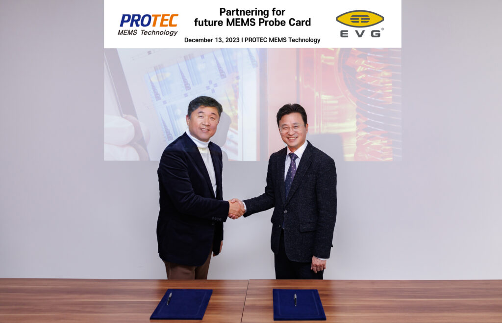
PROTEC MEMS Technology (PMT), one of the leading suppliers of semiconductor wafer probe cards, has ordered a LITHOSCALE® maskless exposure system from EV Group (EVG), a leading supplier of wafer bonding and lithography equipment for the MEMS, nanotechnology and semiconductor markets. Specifically, PMT will install the LITHOSCALE system at its headquarters in Asan-si, Chungcheongnam-Do, South Korea. It will be employed for manufacturing next-generation MEMS-based probe cards for wafer-level testing of advanced NAND, DRAM and High Bandwidth Memory (HBM) devices.
“Fine-pitch probe card manufacturing involves many lithographic patterning steps. These can significantly drive up cost of ownership,” stated Dr. Yong-Ho Cho, CEO of PMT. “We can achieve significant cost savings, faster process development, and improved process performance, by switching from traditional lithography to EV Group’s LITHOSCALE maskless exposure product. We look forward to future collaborations with EVG leveraging LITHOSCALE and other process solutions for advanced probe card manufacturing.”
LITHOSCALE addresses lithography needs for markets and applications that require a high degree of flexibility or product variation. Mainly, it incorporates EVG’s MLE™ (maskless exposure) technology. Thus, LITHOSCALE tackles legacy bottlenecks by combining powerful digital processing that enables real-time data transfer and immediate exposure, high structuring resolution and throughput scalability. It suits rapid prototyping, providing fast turnaround and R&D cycle times.
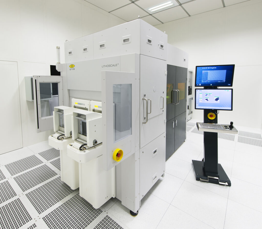
Specifically, MEMS manufacturing poses challenges for lithography due to its complex product mixes, which drive up mask overhead costs. However, LITHOSCALE’s mask-free approach eliminates mask-related consumables. Accordingly, it addresses the demand for low-cost-of-ownership patterning in wafer probe card manufacturing. In addition, LITHOSCALE features high depth of focus and high resolution (sub-2-micron L/S). Specifically, it enables maskless patterning of dense redistribution layer (RDL) and via connections. Thus, it supports technology scaling for fine-pitch probe cards.
According to Young-Sik Yun, general manager of EV Group Korea, “Wafer-level testing with probe cards is an essential process for improving device production yields and reducing overall test cost per die. LITHOSCALE offers a unique combination of high resolution, high flexibility to handle many different product designs, and low cost of ownership. These make it an ideal solution for manufacturing fine-pitch wafer probe cards. We are pleased to support PMT in their efforts to expand their product portfolio and shorten their development cycles.”
- Share:


精密工業第三期工事(正面右奥から真ん中) 完成予想図-150x150.jpg)