ASIA ELECTRONICS INDUSTRYYOUR WINDOW TO SMART MANUFACTURING
Toppan Photomask, IBM Pull New R&D Alliance on EUV
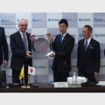
Toppan Photomask Co. Ltd. has entered into a joint research and development agreement with IBM on 2nm logic semiconductor node using extreme ultraviolet (EUV) lithography. In addition, the agreement also includes High-NA EUV photomask development capability on next-generation semiconductors.
IBM and Toppan Photomask will plan and develop photomask capability at the Albany NanoTech Complex in United States and Toppan Photomask’s Asaka Plant in Japan. Accordingly, the agreement will span five years starting Q1 of 2024.
Solutions for 2nm, Beyond
In essence, mass production of 2nm node and beyond semiconductors requires advanced knowledge in material selection. Also, it needs process control that exceeds the requirements of exposure technology using an ArF excimer laser as a light source. For that reason, the IBM and Toppan Photomask agreement brings these essential material and process control skills together. Thus, aiming to provide commercial solutions for 2nm node and beyond printing.
IBM and Toppan Photomask have a long history of technical cooperation. From 2005 to 2015, IBM and Toppan Photomask (then Toppan Printing) jointly developed photomasks for advanced semiconductors. Starting with 45nm node generation, the scope of joint development expanded to 32nm, 22/20nm, and 14nm nodes. Moreover, it also included initial EUV research and development activities. The accumulated technological expertise has contributed to the advancement of the global semiconductor industry.
Since then, Toppan Photomask has continued developing and producing masks and substrate materials for EUV lithography. Additionally, the manufacture of EUV production and next-generation development masks requires advanced multi-beam lithography equipment. Hence, Toppan Photomask is installing several of these systems to meet the latest semiconductor technology roadmap requirements.
Advances IC Miniaturization
Teruo Ninomiya, President and CEO at Toppan Photomask, said, “Our cooperation with IBM is very important for both companies. This agreement will play a crucial role in supporting semiconductor miniaturization, promoting the advancement of the industry, and contributing to the growth of Japan’s semiconductor sector.”
Meanwhile, Huiming Bu, VP of Global Semiconductor R&D at IBM, said, “New photomask capabilities using EUV and High-NA EUV lithography systems will likely play a critical role in designing and producing semiconductor technologies at the 2nm node and beyond. Our collaboration with Toppan Photomask aims to accelerate innovations in advanced logic scaling by developing new solutions to enable advanced foundry manufacturing capabilities, a critical part of the semiconductor supply chain in Japan.”
- Share: