ASIA ELECTRONICS INDUSTRYYOUR WINDOW TO SMART MANUFACTURING
Toray Technology for ICs Results in Better Production
Toray Engineering Co., Ltd. has developed a packaging technology for ultra-thin semiconductor chips. As a result, having a thickness of 3 μm or less.
Reducing the thickness of semiconductor chips results in reduced electrical resistance. Therefore, lowering energy consumption and reducing the size of semiconductor chips.
Challenges in Thin Chips
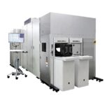
Toray Engineering seeks to commercialize packaging equipment that features this new technology in 2025. That is, to cater to the increasingly widespread use of high-performance semiconductors in power devices, silicon photonics, and memory.
Specifically, in semiconductor packaging, the process of transferring chips from dicing films and other carriers is usually possible using needles.
Chips having a thickness of 100μm or less, as they are thin chips, require special transfer jigs. However, this takes more than 10 times longer than the standard needle method.
On the other hand, the stamp transfer method takes advantage of the differences in adhesive strength. Thus, this has been the preferred method for research purposes. Nonetheless, it requires even more time and comes up against productivity issues.
Proprietary Technology
To overcome these issues, Toray Engineering has developed a new Laser Peel Transfer (LPT) technology. Specifically, it uses the company’s proprietary high-speed and high-accuracy scanning system. Moreover, it picks up and transfers ultra-thin semiconductor chips, which have a thickness of 3µm or less, from the carrier to the substrate.
The process takes place at a speed greater than that of existing flip-chip bonders.
Through its TRENG brand of business solutions that aim to change the world, Toray Engineering utilizes its proprietary technologies, engineering, and know-how to operate wide-ranging businesses, from plant engineering and factory automation systems to semiconductor production and inspection equipment.
Through this new LPT technology, Toray Engineering intends to contribute to the further development of semiconductors and encourage their use in more widespread scenarios, and thereby realize its Corporate Philosophy of “contributing to society through the creation of new value with innovative ideas, technologies and products.”
The new LPT technology was developed based on results obtained from “Research and Development Project of the Enhanced Infrastructures for Post-5G Information and Communication Systems” (JPNP20017), which is subsidized by the New Energy and Industrial Technology Development Organization (NEDO).
-19 April 2024-
- Share: