ASIA ELECTRONICS INDUSTRYYOUR WINDOW TO SMART MANUFACTURING
Intel’s New High NA EUV Makes Chipmaking Breakthrough
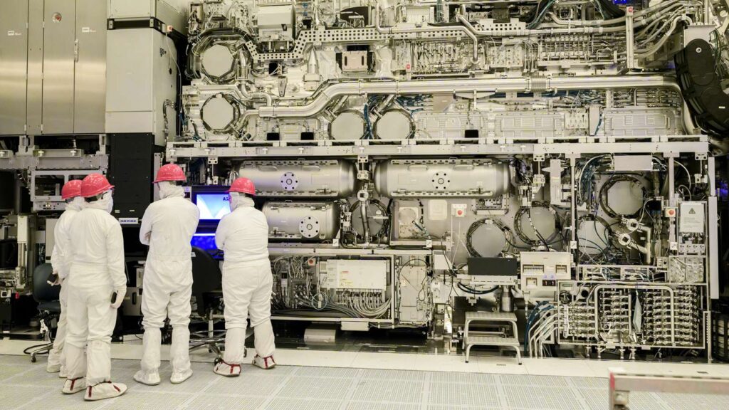
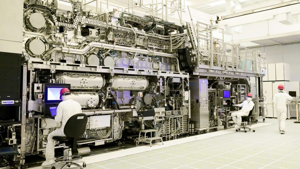
Intel Foundry has made another key milestone in advanced semiconductor manufacturing. This as the company completed the assembly of the industry’s first commercial High Numerical Aperture (High NA) Extreme Ultraviolet (EUV) lithography scanner.
Intel’s TWINSCAN EXE:5000 High NA EUV tool from lithography leader ASML is now going through calibration steps at the company’s Hillsboro, Oregon, R&D site. Accordingly, the company is preparing the system for production of Intel’s future process roadmap.
Most importantly, the new tool can dramatically improve resolution and feature scaling for next-generation processors. This has been made possible by changing the optics design for projecting printed images onto a silicon wafer.
“With the addition of High NA EUV, Intel will have the most well-rounded lithography toolbox in the industry, enabling the company to drive future process capabilities beyond Intel 18A into the second half of this decade,” said Mark Phillips, Intel Fellow and director of Lithography, Hardware and Solutions for Intel Foundry Logic Technology Development
Yields Finest Lines
High NA EUV toolswill play a critical role in advanced chip development and the production of next-generation processors. Intel Foundry, the industry’s first mover on High NA EUV, will be able to deliver precision and scalability in chip manufacturing. Thus, enabling the company to develop chips with the most innovative features and capabilities that are essential for driving advancements in AI and other emerging technologies.
ASML recently announced it has printed the first-ever 10nm dense lines in the High NA lab at the company’s headquarters in Veldhoven, Netherlands. These are the finest lines ever printed, setting a world-record resolution for an EUV lithography scanner. Accordingly, this demonstration validates the innovative High NA EUV optics design from ASML partner Zeiss.
After the tool’s optics, sensors and stages completed coarse calibration, it was able to generate groundbreaking images. Thus, a stepping-stone to running at full specification. ASML’s ability to print 10nm dense lines with a full field optical lithography system is a key step toward readying the High NA EUV tool for commercial use.
Integrating to Intel’s Foundry
When combined with Intel Foundry’s other leading process technology capabilities, High NA EUV will be able to print features up to 1.7x smaller than existing EUV tools. For that reason, 2D feature scaling will be possible, resulting in up to 2.9x more density. Intel continues to lead the way forward for ever-smaller, ever-denser patterning that drives Moore’s Law across the semiconductor industry.
Compared to 0.33NA EUV, High NA EUV (or 0.55NA EUV) can deliver higher imaging contrast for similar features. Thus, enabling less light per exposure reducing the time required to print each layer, and increasing wafer output.
Intel expects to use both 0.33NA EUV and 0.55NA EUV alongside other lithography processes in developing and manufacturing advanced chips, starting with product proof points on Intel 18A in 2025 and continuing into production of Intel 14A. Moreover, Intel’s approach will optimize advanced process technology for cost and performance.
About Intel’s Role
Intel has collaborated with ASML for decades to drive the evolution of lithography from 193nm immersion lithography to EUV, and now to High NA EUV. Thus, the result is the TWINSCAN EXE:5000, one of the most advanced manufacturing tools built.
The adoption of High NA EUV lithography puts the company at the forefront of Moore’s Law scaling, moving the company well into the Angstrom Era.
The TWINSCAN EXE:5000 system made its way to Oregon in more than 250 crates inside 43 freight containers. It had to go through multiple cargo planes before it landed in Seattle, and utilized 20 trucks for the drive to Oregon. Moreover, the total weight of each new system is more than 150 metric tons.
Earlier, Intel announced its plans to adopt High NA EUV in 2021. Then, in 2022, Intel and ASML announced their continued collaboration to drive this advanced technology. Intel plans to acquire the next-generation TWINSCAN EXE:5200B system, with a productivity of more than 200 wafers per hour, making the company an industry first mover on this system as well.
More About High NA EUV
High NA EUV lithography is an evolutionary step beyond EUV lithography, which uses a wavelength of light (13.5nm) that does not naturally occur on Earth. Accordingly, a powerful laser creates the light hitting a droplet of tin heated to a temperature of almost 220,000 degrees Celsius. This is almost 40 times hotter than the average surface temperature of the sun. This light reflects off a mask containing a template of the desired circuit pattern, and then through an optical system built with the most accurate mirrors ever fabricated.
Numerical Aperture (NA) is a measure of the ability to collect and focus light. By changing the design of the optics used to project a pattern onto a wafer, High NA EUV technology enables a significant step forward in resolution and transistor size. Moreover, the ability to create transistors at these smaller dimensions also requires new transistor structures and improvements in other process steps. Currently, Intel is developing this in parallel to the integration of the first High NA EUV system.
–19 April 2024-
- Share: