ASIA ELECTRONICS INDUSTRYYOUR WINDOW TO SMART MANUFACTURING
Onto Innovation Magnifies Wafer Anomaly with New Technique
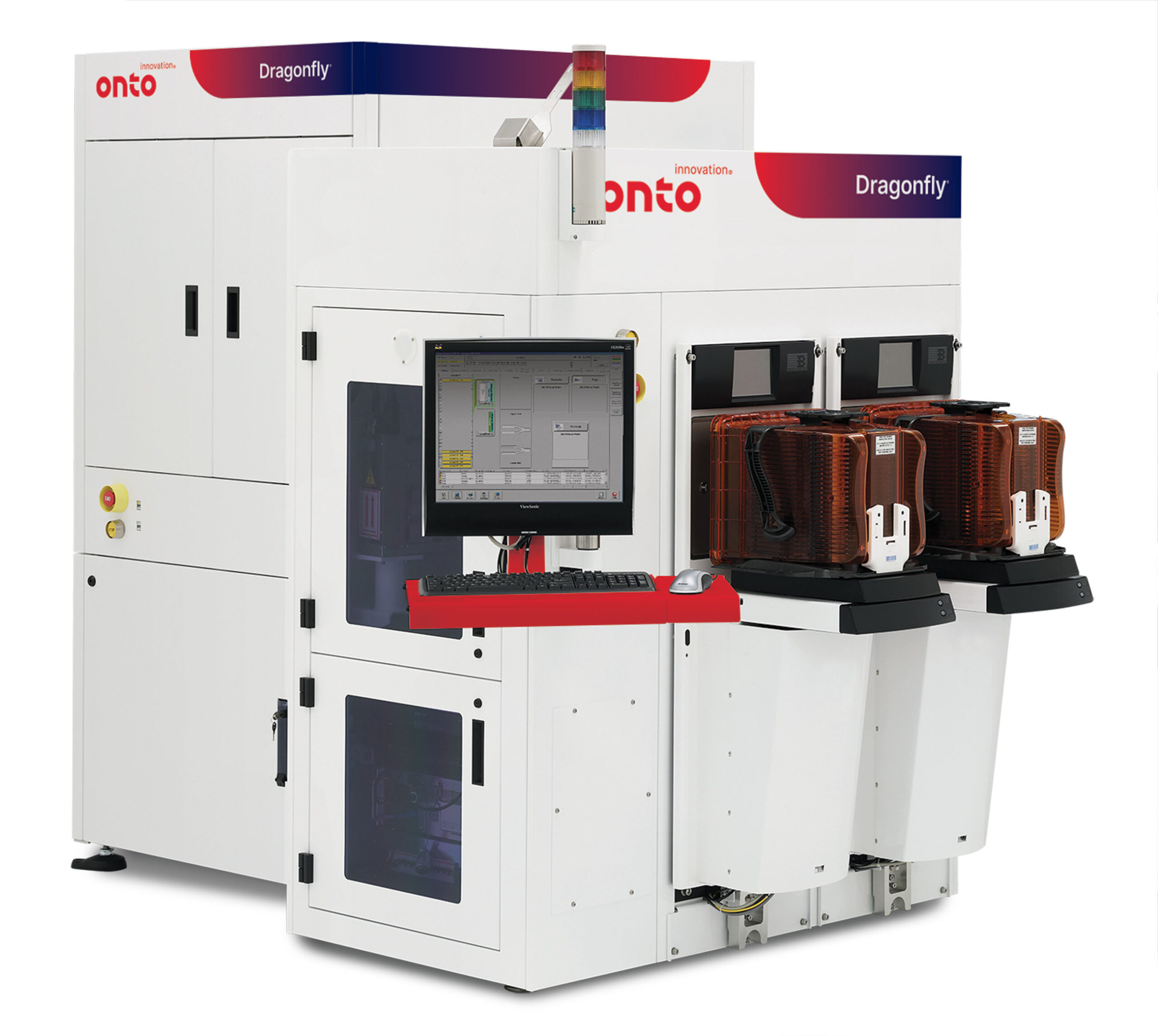
Onto Innovation Inc. has released a new sub-surface inspection capability for the Dragonfly® G3 sub-micron 2D/3D inspection and metrology platform. Primarily, the new capability enables whole wafer inspection for critical yield impacting defects. Accordingly, this leads to lost die as well as entire wafers breaking in subsequent process steps. Such defects were previously impossible to find in a production environment.
In today’s world of wafer thinning and multi-layer wafer or die bonding, sub-surface defects are far more dangerous. Mainly, this results from bonded layers being a tenth of their former thickness and far more brittle. Therefore, they are more susceptible to damage pre- or post-bonding. Sub-surface defects that occur during the bonding or thinning process such as micro-cracks can cause die yield issues. Moreover, they can shatter the wafer resulting in the loss of hundreds of dies in an instant.
Sub-surface Defect Inspection Capability
Now, Onto Innovation is offering the capability to detect these yield-killing defects on the well-established Dragonfly platform at production speeds. The Dragonfly platform uses novel infrared (IR) technology and specially designed algorithms. Thus, it provides customers a choice to scan the entire wafer for hidden defects rather. This compares to sampling only only selected areas of the wafer. This greatly impacts final yield and cost savings through reduced scrapped wafer/die stacks.
“Customers are demanding 100% inspection capability with production-worthy throughput,” says Mayson Brooks, vice president and general manager of Onto’s inspection business. “The Dragonfly G3 system’s new high-speed IR capability delivers just that, combined with the flexibility to select from multiple objective lenses allowing customers to inspect at different magnifications for different applications and devices.”
“The Dragonfly G3 system with its enhanced sub-surface defect detection builds upon the previous model’s successful adoption by HBM customers for die position metrology on stacked dies and wafers,” says Brooks.
According to TechInsights, the market for inspection products supporting wafer-level packaging (WLP) is forecast to grow from $400 million in 2024 to more than $600 million by 2028. The advanced node portion of this market supporting new HBM technologies as well as advanced GPUs used in artificial intelligence (AI) applications is currently outgrowing the overall market with an annual growth rate of >19%.
-25 April 2024-
- Share: