ASIA ELECTRONICS INDUSTRYYOUR WINDOW TO SMART MANUFACTURING
New Equipment Simplifies Chiplet Assembly Process
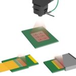
Shin-Etsu Chemical Co., Ltd. has developed new equipment to manufacture semiconductor package substrates. Primarily, it features a new method for manufacturing micro-LED.
The new machine is a high-performance processing equipment using excimer laser. Herein, a dual damascene method is applied to package substrate manufacturing process (back-end process) (Shin-Etsu dual damascene method). It is also used in the front end of semiconductor manufacturing process.
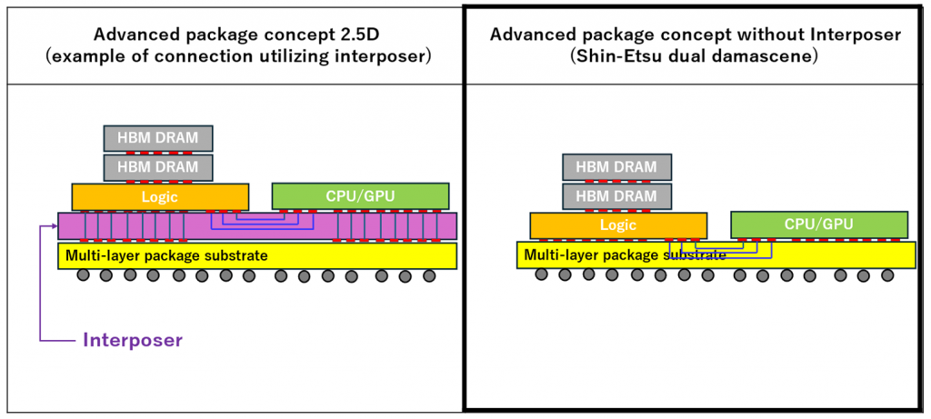
As a result, an interposer’s function is directly formed into a package substrate. Thus, it eliminates the need for interposer. Also, it enables further microfabrication, where conventional manufacturing methods could not realize.
Moreover, it reduces costs and capital investment as it does not require the photoresist process in package substrate manufacturing process.
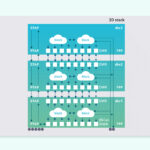
Conventional Chiplet Technology
In a chiplet, circuits are singulated and then assembled in a package. It has caught attention as a technology to reduce the manufacturing cost of higher-performance semiconductors. This technology requires a process to mount several chiplets on an intermediate substrate and connect them. An interposer is the intermediate substrate.
Dual Damascene Method
Eliminates interposer
With the Shin-Etsu dual damascene method, an interposer is no longer necessary. Thus, it significantly simplifies the assembly process. In this method, chiplets are connected to a package substrate with wiring patterns, which has an equivalent function of an interposer.
Consequently, this shortens the assembly process of advanced semiconductors with chiplet technology. Also, it can drastically reduce manufacturing cost.
Direct formation of circuit patterns
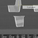
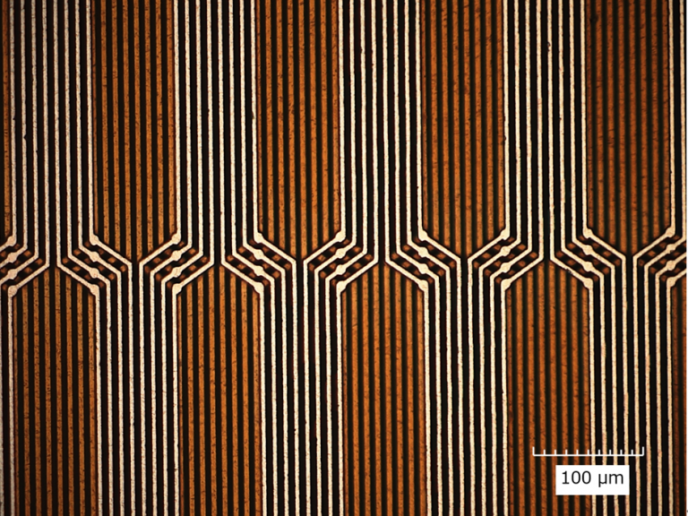
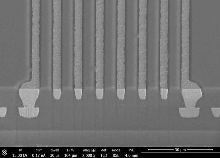
The equipment’s sophisticated microfabrication technology allows complicated electric circuit patterns to be formed directly in each organic insulation layers of a multi-layered package substrate, followed by circuit forming by copper plating. It uses an excimer laser as a light source to form large-area electric circuit patterns in batches.
Furthers microfabrication
The Shin-Etsu dual damascene method enables further miniaturized microfabrication, which could not be achieved by semi-additive processing (SAP) method using dry film resist, as is the current mainstream.
The laser processing equipment can process an area of 100mm2 or larger at one time with a combination of a photomask made of Shin-Etsu’s large photomask blanks and its unique special lens. Processing time varies depending on the size of one package substrate. However, the time necessary to process the wiring pattern and electrode pads is the same as the time to process vias.
Moreover, the via processing time does not depend on the number of vias. For example, it takes about 20 minutes to form trenches of 2µm width and 5µm depth and electrode pads of 10µm diameter and 5µm depth on an organic substrate of 515 × 510mm, as well as to form vias (upper diameter 7µm, lower diameter 5µm, depth 5µm).
Shin-Etsu Chemical is working on initiatives to integrate its own material and equipment technologies. By developing new process technology, it will propose total solutions from the perspectives of both equipment and materials and take the lead in the development of next-generation technologies to create an affluent society.
-13 June 2024-
- Share: