ASIA ELECTRONICS INDUSTRYYOUR WINDOW TO SMART MANUFACTURING
SCREEN Upgrades PCB Direct Imaging System
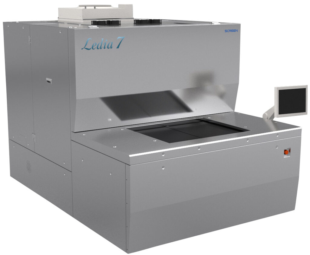
SCREEN PE Solutions Co., Ltd. has developed the new Ledia 7F printed circuit board (PCB) direct imaging system. The system exclusively supports high-definition pattern formation for High Density Interconnect (HDI) substrates and package substrates. Market demand for these substrates is rapidly expanding particularly for 5G and internet of things (IoT) infrastructure.
HDI Substrates Trends
The demand for PCBs mounted on electronic devices has increased recently. The rapid spread of IoT infrastructure centered on 5G-compatible smartphones, tablets, in-vehicle, and industrial equipment appreciated this trend. However, HDI substrates and package substrates are becoming smaller and denser, which is essential to form higher resolution patterns than before. The PCB industry, thus demands direct imaging systems that feature high definition of drawing performance and high productivity.
High-Resolution Model
SCREEN is one of the leaders in direct imaging systems in PCB production. Its system has been recognized as the de facto standard in the solder resists industry. The company has recently developed the high-resolution Ledia 7F, which evolved from the company’s conventional model, Ledia 6F.
Ledia 6F incorporates advanced technology for further improving the imaging position accuracy and renew the exposure section mechanism. By reducing the spot size of the exposed surface by 30 percent, it supports solder resist exposure of high-end package substrates. Also, the higher resolution of the data feeding pitch has made it possible to draw diagonal lines and curves more smoothly. It is a highly versatile device, which can be used for pattern formation with high aspect ratios, such as metal masks and electronic components.
The company will continuously accelerate business development in the HDI and package board market by expanding the lineup of the Ledia Series to meet the expansion of 5G and IoT infrastructure.
