ASIA ELECTRONICS INDUSTRYYOUR WINDOW TO SMART MANUFACTURING
LEM to Boost Tech Growth With More R&D Sites
Electrical measurement technology specialist LEM has opened new research and development facilities in Munich and Shanghai.
Accordingly, the move aims to satisfy the growing global demand for current and voltage sensing. Moreover, to meet the global drive towards decarbonization and greater electrification
The two new sites will enable LEM to build greater intelligence into its sensors. In addition, to have development bases closer to key customers. At the same time, to promote deeper collaboration on projects and the efficient sharing of vital product design information.
Boost IC Design, Production
The China site will have the latest laboratory equipment. On the other hand, the site in Germany will focus on application-specific integrated circuit (ASIC) design and semiconductor technology. Thus, will help accelerate LEM’s innovation in integrated current sensors (ICSs).
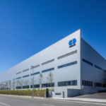
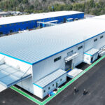
This latest investment in additional R&D facilities in Europe and Asia follows from LEM’s recent inauguration of a state-of-the-art factory in Malaysia. LEM’s investment in the state of Penang is an acknowledgment of the region’s expertise in ASIC technology and its specialization in semiconductor design and production.
The Penang factory is the latest example of LEM’s quest to secure its operations. At the same time, diversifying its global footprint so that it could serve customers better through a combination of advanced production facilities and skilled personnel.
Formidable R&D Activities
LEM is now backing up this significant investment in production capacity and flexible delivery with R&D capabilities. Specifically, to complement the existing site in Lyon (France), which opened in 2017. Moreover, the company aims to build up further on R&D activities.
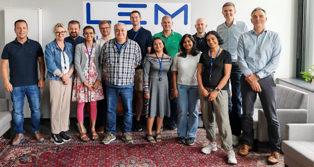
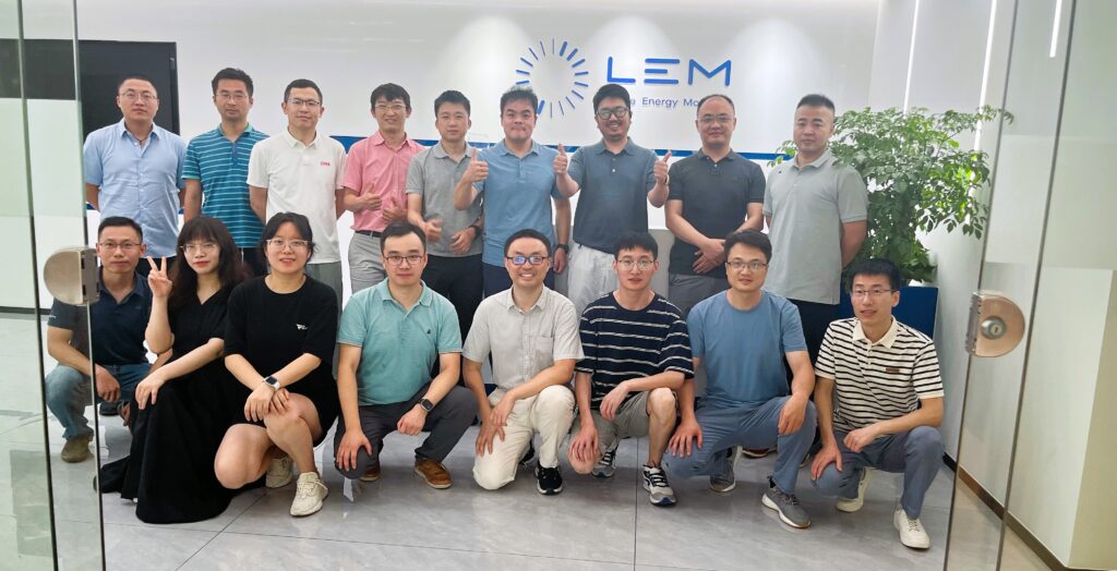
Led by Matthias Tänzer, the development team at the new Munich semiconductor facility will work closely with LEM’s existing ICS team in Geneva, Switzerland. There are already 10 employees in place at Munich and this number will increase in line with LEM’s ambitious growth plans for the site. At the site of the 1,400sq.m Shanghai facility, there are currently 30 staff with the capacity to more than double that number in the future, many of whom will be involved in R&D.
LEM CTO Verena Vescoli says, “As a leader in electrical measurement, we strongly believe that integrated current sensing is a critical part of our future growth. It is vital that we have an ICS offering that can meet our customers’ needs. The new R&D center in Munich will enable us to accelerate on IC design and enable a broad ICS portfolio.”
In addition, Vescoli says, “It is always a delight to see multiple teams working together to share the depth of their ICS design expertise and application know-how. I am very excited by the potential for growth that the new Munich and Shanghai sites will offer.”
27 August 2024
- Share: