ASIA ELECTRONICS INDUSTRYYOUR WINDOW TO SMART MANUFACTURING
New Inspection Observes OLEDs at Ultra-low Brightness
Toyo Technica Co., Ltd. announces it has developed a new inspection technology to investigate the behavior of OLED devices at ultra-low brightness. Mainly, this development was made with TOYOTech LLC, its subsidiary in the U.S., Sharp Display Technology Co., Ltd., and the Japan Advanced Institute of Science and Technology.
Primarily, this technology quantifies the difference between the voltage at which current begins to flow rapidly in an OLED element, and the light-emitting start voltage as the element deteriorates. It is useful for analysis of deterioration and display unevenness at low brightness in OLED elements that require long life. They jointly presented this technology at the International Meeting on Information Display held in Korea in August.
On October 1, 2024, TOYOTech will launch the “DCM1000 DC-JVL Measurement System” in the United States, Japan, and other Asian and European countries.
Background/Overview
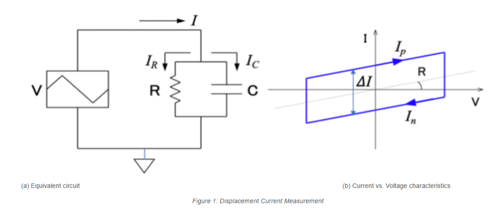
The formation of organic electroluminescence*1 devices involves stacking thin films of several tens of nanometers in length in multiple layers. Characterization is performed to optimize the deposition conditions of these thin films. In this characterization, it is common to simultaneously measure the current flowing through the element and the luminance*2 while applying a voltage called the J-V-L (Current Density-Voltage-Luminance) characteristic. However, with the J-V-L characteristics, it was not possible to measure the minute current and low brightness at the start of light emission of the device due to the limitations of the sensitivity of the device.
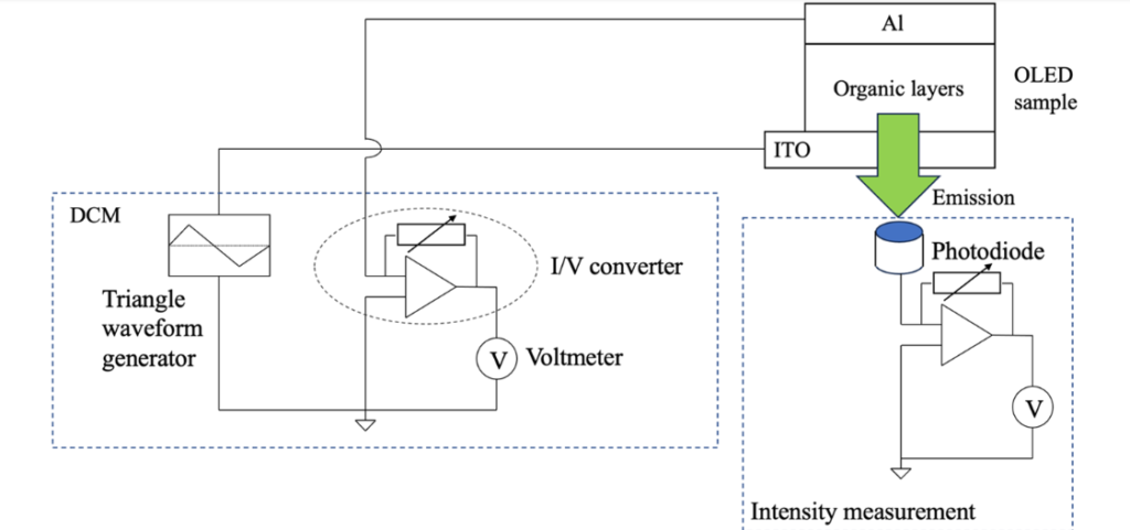
In this newly developed technology, the minute current (displacement current) flowing through the OLED element and the emission intensity of the light emitted by a high-sensitivity silicon photodiode are measured simultaneously. Accordingly, the difference between the voltage at which the sudden current change occurs and the voltage at which the light starts is detected and analyzed. In addition, it is possible to consistently measure ultra-low brightness and current, and luminous intensity at high brightness while constantly optimizing the range.
Primarily, this technology can analyze display unevenness caused by deterioration of OLED elements. Also, it can contribute to further improvement of the performance of OLED elements.
・Product page: https://toyotechus.com/lab-dcm1000/ (on the TOYOTech website)
*1 A luminescence phenomenon that occurs when a voltage is applied to an organic compound (organic EL element). By using this phenomenon, it is possible to realize a thin, light, and low-power displetion in TVs and smartphones. Since the OLED element itself emits light and emits color, the structure is simpler than that of liquid crystal displays.
*2 The degree of brightness of the light emitted from the OLED element. The unit is cd/m2 (candela per square meter )
This is an online translation of a Japanese press release with slight editing made by Dempa.
-10 September 2024-
