ASIA ELECTRONICS INDUSTRYYOUR WINDOW TO SMART MANUFACTURING
Resonac Develops New Temporary Bonding Film
Resonac Corporation has developed a temporary bonding film to support a wafer on a glass carrier temporarily in the semiconductor device fabrication process (front-end process) and semiconductor packaging process (back-end process). Additionally, it developed the debonding process for the temporary bonding film.
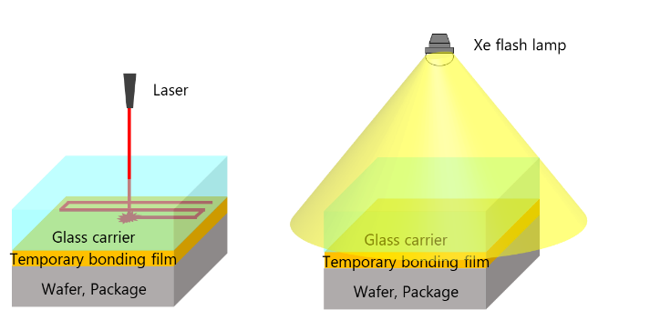
Specifically, this debonding process uses xenon (Xe) flash light irradiation to debond the wafer or package from the carrier. It can be applied from wafer level to panel level processing. Also, the debonding is completed faster compared to conventional laser ablation method without producing foreign substances such as soot. This technology has been patented in Japan, the United States, Korea, China, and Taiwan region.*
Presently, Resonac is looking for development partners to establish a new debonding process and market the new temporary bonding film.
Temporary Bonding Film Improves Workability
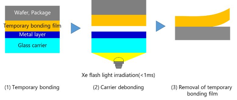
In the front-end and back-end processes of advanced semiconductors, wafers and chips are temporarily bonded to a glass carrier with a temporary bonding material to improve workability. After various fabrication processing, the wafers or packages are debonded from the carrier along with the temporary bonding material. Therefore, the performance of the temporary bonding material must be compatible with all fabrication processes.
Moreover, the residual temporary bonding material must be easily removed. Additionally, debonding process must be completed in a short time without damaging them to achieve high yield and productivity. Furthermore, even the back-end process is now required to be as clean as the front-end process. Therefore, the soot, which is generated by the conventional laser ablation debonding method, has not been preferable.
Sufficient Adhesion Performance
Resonac’s temporary debonding film features high heat resistance and chemical resistance. Thus, it exhibits sufficient adhesion performance when wafers and packages are temporarily supported on the carrier. Once they are debonded from the carrier, the film can be removed easily by peeling at room temperature without any residues.
Specifically, the process for debonding the wafer from the carrier adopts Xe flash light irradiation, which allows for large-area batch irradiation and instantaneous high energy output. Instant deformation induced by locally heating a metal layer on the glass carrier with Xe flash light irradiation enables quick debonding of wafers and packages without applying heat or mechanical stress. In addition, as the debonding mechanism is not related to resin decomposition, this method has the advantage of being a clean process that does not generate any foreign substances, such as soot generated during laser ablation.

Resonac believes that this temporary bonding film and new debonding method are suitable for the fabrication process for memory, logic, and power semiconductors as well as advanced semiconductor packages.
Resonac will continue to contribute to technological innovation in the semiconductor area through co-creation.
*Japan patent No. 7196857, U.S. patent No. 11840648, Korea patent No. 10-2513065, China patent No. ZL201880077311.4, Taiwan patent No. I805655, etc.
-20 September 2024-
- Share: