ASIA ELECTRONICS INDUSTRYYOUR WINDOW TO SMART MANUFACTURING
KLA Unveils New Solutions in Advanced IC Packaging Era
KLA Corporation introduces the industry’s widest breadth of process control and process-enabling solutions for IC substrate (ICS) manufacturing. Primarily, KLA’s combined expertise in front-end semiconductors, packaging, and IC substrates will help customers achieve breakthroughs in packaging interconnect density for chips targeting high-performance applications.
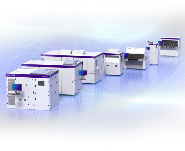
Advanced packaging continues to adopt heterogeneous integration methods to bring together multiple semiconductor components for performance, power, and cost benefits. To meet evolving interconnect requirements, innovation is accelerating for panel-based intermediate packaging levels like IC substrates and interposers.
Particularly, these technologies are used to efficiently connect chips and printed circuit boards (PCBs). As package dimensions increase, feature sizes decrease and novel materials such as glass are introduced. Thus, manufacturers can leverage KLA’s solution portfolio to achieve higher yield, accelerate delivery cycles, and improve overall profitability.
Optimizing Advanced Packaging Workflow
Mainly, KLA’s comprehensive portfolio of direct imaging (DI), defect inspection, shaping, metrology, chemistry process control, and intelligent software solutions optimizes the advanced packaging manufacturing workflow.
Corus direct imaging platform
Primarily, KLA’s portfolio includes multiple direct imaging solutions supporting a range of customer lithography requirements. Specifically, market adoption of the Corus™ direct imaging platform demonstrates its proven capability in providing a highly flexible and efficient imaging solution. Thus, to meet evolving needs for applications like IC substrates and next-gen high-density interconnect (HDI), the capability is being extended with next-generation optics and lasers. This aims to optimize dynamic imaging and layer-to-layer accuracy at speed, even for varying panel topographies.
Serena direct imaging platform
For advanced IC substrate applications, direct imaging represents a new category beyond steppers for lithography. KLA is introducing the new Serena™ direct imaging platform for quality, finer line patterning of large-sized, high-layer count organic substrates for increased accuracy and yield with the efficiency of a flexible digital solution.
Lumina inspection and metrology system
Meanwhile, Lumina™ new inspection and metrology system for advanced IC substrates (including glass core) and panel-based interposers, enables high-sensitivity detection and scanning metrology at optimized cost of ownership. Specifically, the system delivers monitoring paired with AI-based review and classification for an actionable defect Pareto chart without the need for operator input, as well as a seamless integration with KLA’s copper-shaping solutions.
Process control solutions
Further, the portfolio is strengthened with proven KLA process control solutions featuring the Orbotech Ultra PerFix™, EcoNet™, Zeta™-6xx, ICOS™ T890, Quali-Fill® Libra® and QualiLab® Elite product lines. KLA’s Frontline software solutions span engineering, computer-aided manufacturing (CAM), and production data analytics to centralize and apply intelligence throughout IC substrate manufacturing, building on KLA’s longtime leadership in yield management.
“With today’s portfolio news, KLA is affirming our leadership in semiconductor ecosystem innovation,” said Oreste Donzella, executive vice president and chief strategy officer, KLA Corporation. “IC substrates and other panel-level packaging technologies are essential to advancing connectivity within tomorrow’s high-performance chips. To this end, KLA is collaboratively engaged with customers in solving complex production challenges to maximize their yield and business success.”
-17 October 2024-
