ASIA ELECTRONICS INDUSTRYYOUR WINDOW TO SMART MANUFACTURING
New Method Lets 3D Integration of Thin-Film Analog IC
OKI Electric Co., Ltd., in collaboration with Nisshinbo Micro Devices Co., Ltd., has successfully adopted CFB® (Crystal Film Bonding) technology (Note 1) to integrate thin-film analog ICs (Note 2) three-dimensionally (Note 3). Primarily, this technology can be applied to heterogeneous integration (Note 4), which integrates various semiconductor devices such as analog ICs. Both companies will proceed with product development using this technology, aiming for mass production in 2026.
In recent years, with the spread of AI and autonomous driving, the need for even more sophisticated semiconductor devices has increased. Amid this trend, chiplet technology (Note 5) has been attracting attention. Mainly, chiplet technology does not integrate all functions into a single chip. Instead, it divides each function into small chips and integrates them using 2.5-dimensional and 3-dimensional mounting technology. This realizes large-scale functional integration at low cost and in a small area. In addition, by dividing the parts, yields are improved. Moreover, the optimal semiconductor manufacturing process can be selected to realize each function, thereby suppressing cost increases.
Challenges in Applying Chiplet to 3D Integration
Mainly, there are two main challenges in applying conventional chiplet technology to 3D integration of low-end analog ICs:
The first challenge is the development of 3D integration technology that can be handled using legacy processes (Note 6). Particularly, 3D integration greatly contributes to increased integration and miniaturization because chips are stacked vertically. However, TSV (Through Silicon Via) technology (Note 7) is generally used to electrically bond stacked chips together, which requires capital investment and advanced process development. This makes traditional techniques an expensive process.
The second challenge is the prevention of noise (crosstalk noise) caused by interference with electrical signals. Analog ICs have meaning for the entire continuous signal change, not just “0” and “1”, and handle signals with higher voltages compared to digital ICs. Therefore, when the circuit layers of the IC are close together due to stacking, crosstalk noise increases.
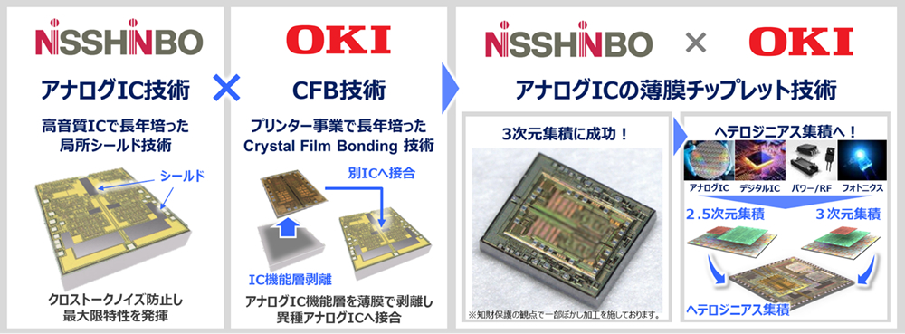
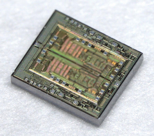
This time, OKI has developed a new “thin film chiplet technology” to solve the first problem. This technology consists of a CFB process of peeling and bonding, followed by rewiring. First, the functionality of the analog IC is completely protected. Also, only the functional layer of the analog IC is removed from the substrate.
By bonding this thin film analog IC onto a different analog IC, the company enables 3D integration of thin film analog ICs. In the case of three-dimensional integration using general TSV, the thickness of the IC chip is tens to hundreds of micrometers, but the thickness of thin film analog ICs bonded using this technology is extremely thin with only a few micrometers. Note 8) Also, rewiring is possible. Rewiring using this technology enables the application of common and inexpensive legacy processes.
To solve the second issue, OKI applied Nisshinbo Micro Devices’ proprietary local shielding technology to analog ICs. Particularly, this technology suppresses signal interference without degrading circuit functionality by shielding only specific areas between the upper and lower chips that are affected, rather than the entire chip. This time, the company has developed this technology by leveraging the low-noise analog IC technology it has cultivated over many years in high-quality sound ICs. Accordingly, it has succeeded in verifying normal operation by suppressing crosstalk noise even under high voltage output of 20Vpp.
The successful 3D integration of thin film analog ICs, co-created by Nisshinbo Microdevices Corporation and OKI, makes it possible to provide analog solutions by combining with various analog ICs. In addition, by applying OKI’s “thin film chiplet technology” to the heterogeneous integration of various semiconductor devices such as digital, analog, optical, power, and sensor devices, it will contribute to the new evolution of semiconductor devices.
Going forward, the two companies will continue to develop products with new added value using this technology. Particularly, they target mass production in 2026 with an eye toward partnership and licensing.
A demonstration of this technology will be held at OKI WORLD 2024. It will happean at Bellesalle Tokyo Nihonbashi from October 23rd to 24th, 2024. A detailed explanation will also be given at a seminar at the exhibition.
Terminology
Note 1:CFB (Crystal Film Bonding) Technology
OKI’s proprietary technology for thin film peeling of the functional layer of a semiconductor device and bonding it to different material substrates by intermolecular force. Since it is a direct bonding that does not involve adhesives, electricity, light, heat, etc. can be propagated between bonds, and semiconductor processing after bonding is possible, contributing to the creation of new semiconductor devices that integrate different materials and functions.
Note 2: Analog ICs
An integrated circuit that has processing functions to amplify, filter, and convert continuously changing analog signals such as sensors.
Note 3: Three-dimensional integration
A technology in which semiconductor devices are stacked vertically and electrical connections are made between layers.
Note 4: Heterogeneous agglomeration
A technology that combines and integrates different semiconductor devices, such as different process nodes (generations of microfabrication technology), different functions (digital ICs, analog ICs), and different semiconductor materials (optical devices, next-generation semiconductors).
Note 5: Chiplet technology
This is a technology that divides a single-chip semiconductor device into multiple small chiplets and integrates them using mounting technology. As a result, it is possible to improve the yield in large-scale production by increasing functionality.
Note 6: Legacy Processes
A semiconductor manufacturing method that uses the manufacturing technology and equipment of the previous generation. It is still used in many semiconductor processes today due to its stability, reliability, and cost-effectiveness.
Note 7: TSV (Through Silicon Via) Technology
A technology that realizes electrical connections between semiconductor chips in the vertical direction by forming a through-electrode perpendicular to a silicon substrate.
Note 8: Semiconductor lithography
In semiconductor processing, a technology that uses light and electron beams to form extremely fine circuit patterns on a semiconductor substrate.
This article is an online translation of a Japanese press release with slight editing made by Dempa.
-22 October 2024-
- Share: