ASIA ELECTRONICS INDUSTRYYOUR WINDOW TO SMART MANUFACTURING
Fraunhofer, DIVE to Soar Efficient Chip Making
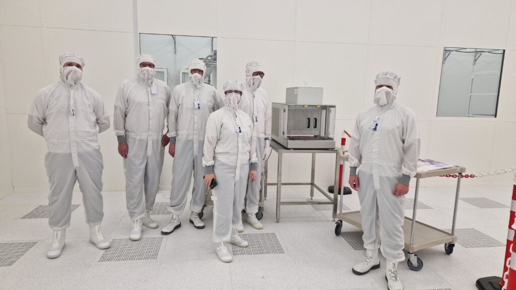
The Fraunhofer Institute for Photonic Microsystems IPMS, in collaboration with DIVE imaging systems GmbH, has achieved a major milestone for a more resource-efficient semiconductor manufacturing.
Specifically, the collaboration led to the successful installation of an optical measurement system of DIVE in the cleanroom of Fraunhofer IPMS. This endeavor contributed to the significant reduction in the effort of ensuring quality control during wafer production. Therefore, Fraunhofer IPMS and DIVE see this collaboration will pave the way for a more sustainable and efficient semiconductor production process.
Material, Energy Resources in Wafer Production
Without a doubt, semiconductor manufacturing involves tedious processes. In fact, it involves approximately 1,500 process steps, which includes etching, deposition, and lithography.
Due to their complexity of structures, finished wafers must be nearly defect-free, which requires rigorous quality control. As a result, up to 50 percent of the process steps are dedicated to metrology and thousands of additional control wafers are produced each month. This requires substantial additional financial and material expenditures as well as energy and time resources.
These challenges in semiconductor manufacturing are among the reasons why the Green ICT Project for New Screening Tool for Efficient Semiconductor Manufacturing (NEST) was established. The project is coordinated by the office of the Fraunhofer Group for Microelectronics and the Research Fab Microelectronics Germany (FMD).
Over the past 1.5 years, DIVE, together with Fraunhofer IPMS and Fraunhofer IZM has conducted an environmental potential analysis. The study revealed that targeted inspection tools could reduce control wafer usage by at least 25 percent, while also saving more than 118,000 kilograms of CO₂ emissions during production every month.
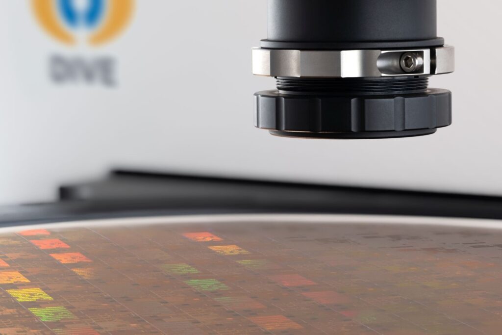
DIVE imaging systems GmbH develops advanced inspection tools that combine the benefits of optical spectroscopy with imaging. The DIVE VEpioneer is the first of its kind to operate under cleanroom conditions. It rapidly assesses surface properties, contamination and deviations from production specifications in just 20 seconds. The integration of AI algorithms enables comprehensive process control while significantly reducing testing efforts.
Moreover, DIVE’s solution uses an innovative combination of spectroscopy and imaging technologies capable of identifying defects even in deeper wafer layers. The analysis was based on a 28nm manufacturing process and 25,000 wafer starts per month. The project was funded within the Green ICT Space by the Research Fab Microelectronics Germany (FMD).
In addition to CO₂ savings, the system offers further ecological benefits, such as the reduction of water and chemicals used in control wafer production. Furthermore, the reduction of metrology steps also improves energy efficiency by freeing up tool capacity; an early detection of process deviations avoids misproduction and improves the overall productive wafer yield, which results in an economic advantage as well.
17 July 2025
- Share: