ASIA ELECTRONICS INDUSTRYYOUR WINDOW TO SMART MANUFACTURING
Samsung Debuts 2.5D Packaging Solution "H-Cube"
Samsung Electronics has developed a new breakthrough packaging technology in what’s called as Hybrid-Substrate Cube (H-Cube) technology.
The latest and most advanced in its 2.5D packaging solution is designed to pack together upward of 6 different dies in a same package.
The H-Cube is a successor to Samsung’s I-Cube 2.5D interposer chip packaging technology
The so-called heterogeneous integration will allow chip makers to integrate CPUs, GPUs, memory chips, sensors and other discrete dies in a single package to power HPC, AI, data center, and network products that require high-performance and large-area packaging technology.
The H-Cube solution is jointly developed with Samsung Electro-mechanics (SEMCO) and Amkor Technology to produce high-performance semiconductors that need to integrate a large number of silicon dies
H-Cube Structure and Features
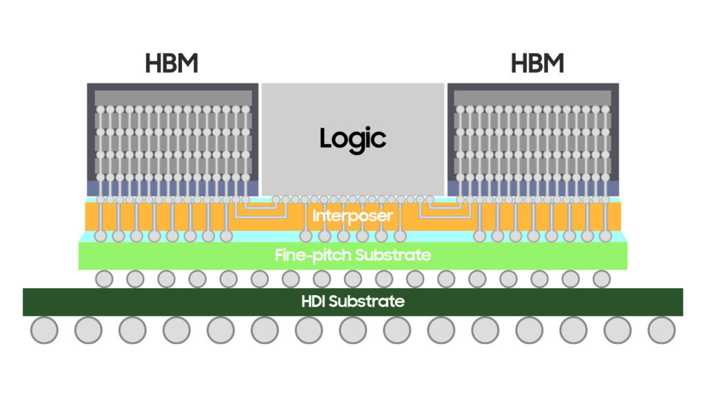
The 2.5D packaging enables logic chips or high-bandwidth memory (HBM) dies to be placed on top of a silicon interposer in a small form factor.
Samsung’s H-Cube technology features a hybrid substrate combined with a fine-pitch substrate which is capable of fine bump connection, and a High-Density Interconnection (HDI) substrate, to implement large sizes into 2.5D packaging.
With the recent increase in specifications required in the HPC, AI, and networking application market segments, large-area packaging is becoming important as the number and size of chips mounted in one package increases or high-bandwidth communication is required.
For attachment and connection of silicon dies including the interposer, fine-pitch substrates is essential but prices rise significantly following an increase in size.
- Share: