ASIA ELECTRONICS INDUSTRYYOUR WINDOW TO SMART MANUFACTURING
Infineon Brings 300mm GaN Power Chips to Volume Production
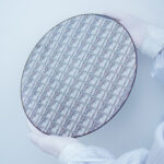
German semiconductor company Infineon Technologies AG plans to establish what it describes as the world’s first high-volume manufacturing facility for gallium nitride (GaN) power semiconductors on 300-millimeter wafers, marking a significant step in scaling next-generation power electronics for industrial and infrastructure markets.

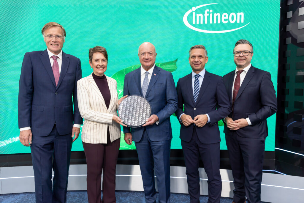
The company said it will invest approximately €1.1 billion in its existing Villach, Austria, facilities through 2034, with production expected to begin by the end of 2027. The expansion is supported by €319 million in funding approved under the European Chips Act.
The project moves Infineon’s 300mm GaN technology from a development milestone into commercial manufacturing. Two years ago, the company announced successful processing of 300mm GaN wafers. It now intends to use the technology for volume production serving customers across multiple sectors.
“By establishing high-volume manufacturing on 300-millimeter wafers, we will be the first company in the world to bring gallium nitride power electronics into volume production,” said Jochen Hanebeck, CEO of Infineon Technologies AG.
He added that the facility is intended to support broader adoption of GaN technology in applications including artificial intelligence, energy infrastructure, e-mobility and robotics.
Manufacturing Economics and Market Demand
According to Infineon, manufacturing on 300mm wafers provides significant efficiency advantages over 200mm production because the larger wafer diameter yields approximately 2.3 times more chips per wafer.
The company said the investment is being driven by growing demand for high-performance and energy-efficient power supply solutions. GaN devices enable more efficient power conversion while reducing energy losses and heat generation, allowing smaller and more powerful electronic systems.
Infineon identified AI data centers, energy infrastructure, electric mobility, robotics and consumer electronics among the key markets expected to benefit from wider GaN adoption.
Strengthening Europe’s Semiconductor Position
Beyond manufacturing capacity, the project is intended to reinforce Europe’s semiconductor ecosystem and reduce dependence on external supply regions for critical semiconductor technologies.
“The entire Austrian semiconductor ecosystem benefits – from research organizations and universities to industrial partners,” said Sabine Herlitschka, CEO of Infineon Technologies Austria AG. “We are thus sustainably strengthening Europe’s competitiveness and strategic autonomy in microelectronics.”
The Villach site already functions as a key center for power electronics research, development and manufacturing within Infineon’s global network. The new facility is expected to create additional synergies with existing R&D activities located at the site.
The investment also strengthens Villach’s role as a global competence center for power semiconductors and advanced semiconductor materials, while positioning Europe more prominently in a market that Infineon said is expected to expand significantly over the coming years.
28 October 2026
- Share: