ASIA ELECTRONICS INDUSTRYYOUR WINDOW TO SMART MANUFACTURING
Panasonic Gives Weight on New IC Process Technologies
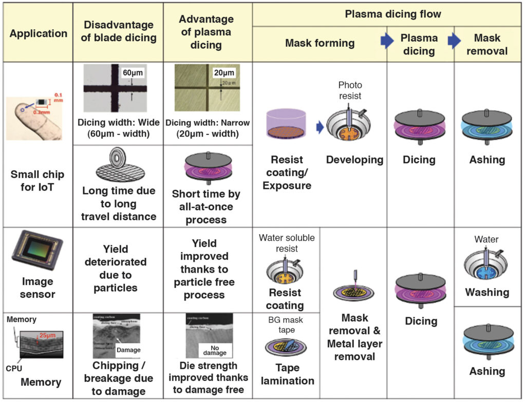
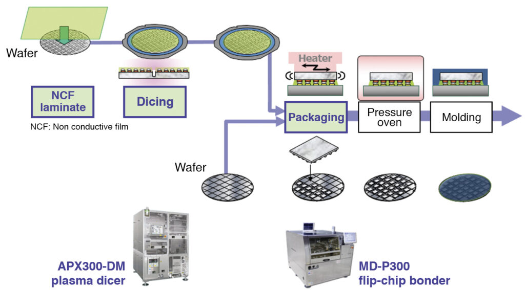
With the advancement of semiconductor devices, wafers have become thinner and more brittle, and chips have become smaller.
These changes have made limits on existing dicing method even more apparent, such as increases of chipping of dies, processing time and materials loss. The dicing is a process to individualize the wafer into dies.
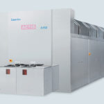
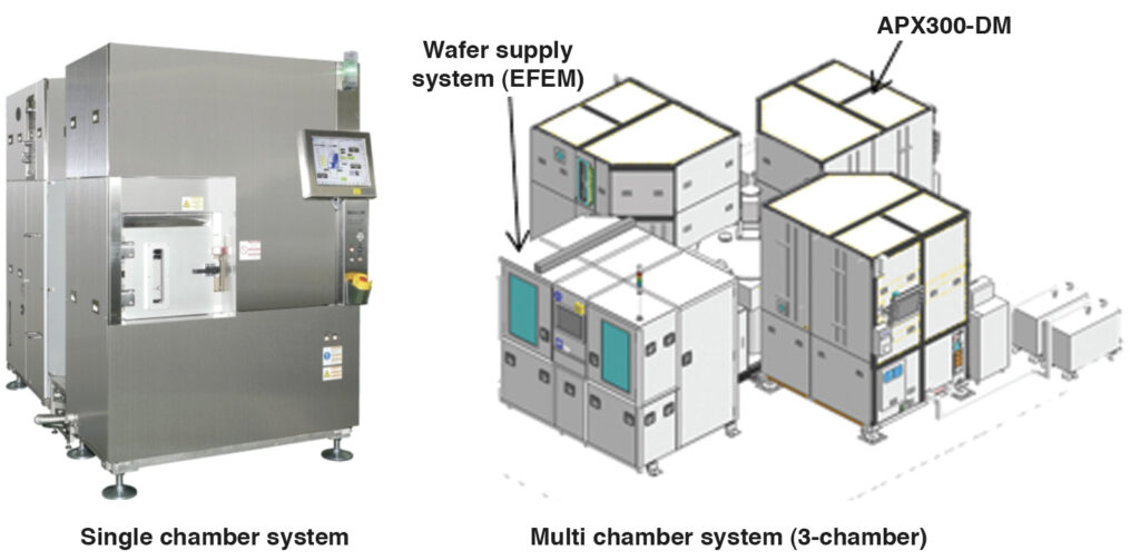
APX300-DM Plasma Dicer
Solving this issue is Panasonic Corporation’s plasma dicing method and system. Panasonic has developed and put to practical use original process technologies for optimal plasma dicing that suit respective hardware and device structures. The plasma dicing system enables plasma processing of wafers without damaging tapes and ring frames
Table 1 shows flows of the plasma dicing process for representative devices.
Features of APX300-DM plasma dicer
Among the features of the APX300-DM plasma dicer include damage-free processing contributes to improved die strength.
Dicing with narrow width/free die shapes result in larger number of dies produced from a wafer.
Furthermore, single or multi chamber system is also available in accordance with production scale.
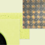
APX300-S Dry Etcher
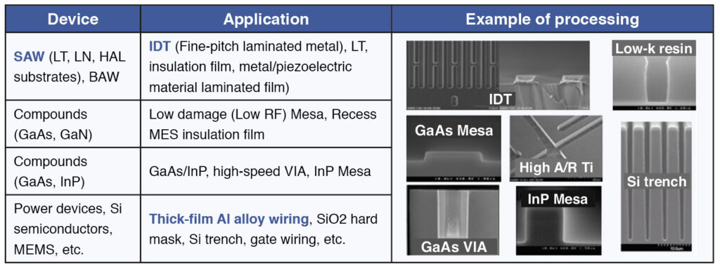
With the advancement of high-frequency communications, the radio frequency (RF) module market has expanded. Various frequency bands use surface acoustic wave (SAW) devices as filters. Normally, the use of dry etching forms comb-shaped electrodes or interdigital transducer (IDT), which determine the frequency of SAW devices.
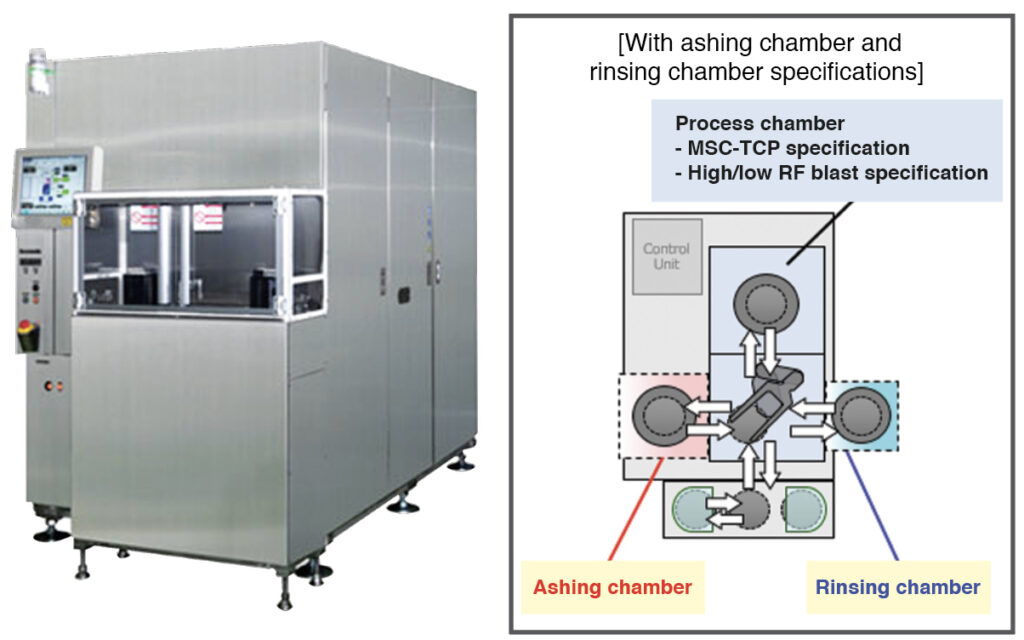
The processing of IDT requires high dimensional controllability for fine aluminum (Al) and metal wirings, a low-damage technology for substrate, and anti-corrosion treatment technology without thermal damage on pyroelectric and various boned substrates. Panasonic’s dry etching system employs multispiral coil inductively coupled plasma (MSC-ICP) plasma source, which realizes high-precision and low-damage processing. Also, it incorporates an ashing chamber and a rinsing chamber inline, thereby achieving low-temperature anti-corrosion processing. Panasonic can provide integration of etching, ashing and rinsing technologies for compound semiconductors, power devices, and micro electromechanical systems (MEMS) as well, in accordance with process applications, such as metal wiring processing.
Features of APX300-S single wafer processing dry etcher
The APX300-S single-wafer-processing dry etcher has a track record of mass producing many wafers for power devices, communications devices, and MEMS sensors.
It comes equipped with ashing and rinsing functions, realizing processing without residue and corrosion.
Furthermore, faraday shield-inductively coupled plasma (ICP) (expanded function) enables stable processing of nonvolatile materials.
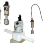
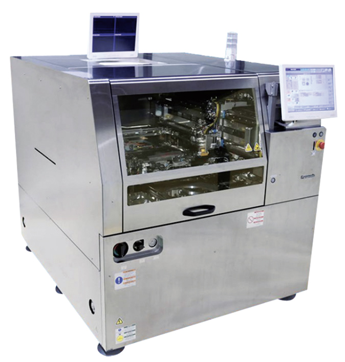
NCF-US Process, MD-P300 Ultrasonic Flip-Chip Bonder (Sample exhibition)
Panasonic has been proposing the non-conductive film (NCF)-ultrasonic (US) process, which is a revolutionary process, taking the lead in the packaging industry.
With the proliferation of fifth-generation (5G) communications, the number of inputs/outputs (I/O) of application processors (APs) and memories have increased and their pitches have become narrower to achieve high-speed, large-capacity communications. As a result, improvements in accuracy of flip-chip packaging using thermal-compression bonding method and improvement of productivity have emerged as issues.
Panasonic proposes NCF-US bonding as a new process that overcomes the low productivity of the thermal-compression bonding method. The thermal-compression bonding method takes a long process time with a mounting tact of about 10 seconds. Panasonic’s NCF-US bonding method uses ultrasonic waves and features high accuracy and process time of one second or shorter. As a result, this method achieved mounting tact of about 2 seconds and significant improvement of productivity.
Features of MD-P300 high accuracy specification ultrasonic flip-chip bonder (Sample exhibition)
The MD-P300 ultrasonic flip-chip bonder comes with high-accuracy packaging at +/-3μm (3σ). It also has high-speed packaging of 1.0s/IC, excluding process time.
Furthermore, the flip-chip bonder comes with significant improvement of productivity through process innovation and is also compatible with φ300mm CoW.
- Share:


About This Article:
The author is Shinji Sasaguri, Manager, Circuit Formation Processes Solution & Sales Coordination Department, Semiconductor & FPD Marketing Department, Semiconductor Process Section, Customer Success Core Center, Panasonic Smart Factory Solutions Co., Ltd.