ASIA ELECTRONICS INDUSTRYYOUR WINDOW TO SMART MANUFACTURING
Bump Support Film Improves Reliability of WLCSP
As mobile communication devices such as smartphones, tablet computers, and wearable devices are becoming widely used, market demand for communication IC chips has seen to increase. The wafer-level chip size package (WLCSP) process is commonly used for the said devices because of its manufacturing cost advantage. As the performance of packages is being improved, IC chip sizes for the WLCSP process will probably expand.
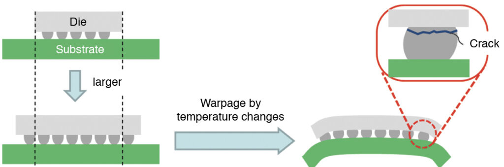
However, increasing chip sizes will also increase the warpage of chips, and raise the risk of cracks forming in solder joints (Fig. 1). LINTEC Corporation, therefore, is proposing the use of Bump Support Film (BSF) as a protective material for bumps. This article describes the group’s BSF.
BSF Process
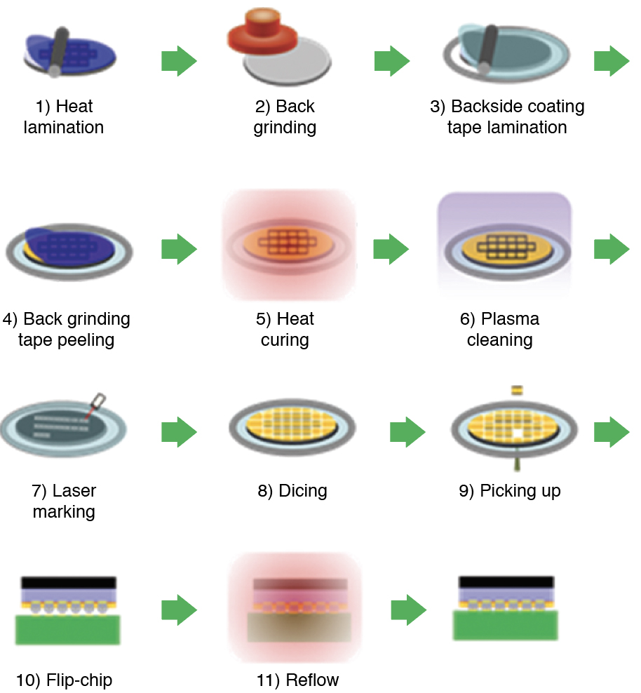
The BSF consists of back grind (BG) tape and a stacked Bump Support Layer (BSL), and the company proposes a manufacturing process as presented in Fig. 2. First, the BG tape and the stacked BSL are laminated by heat on the bump formation surface, and back grinding is performed. Then, a backside coating tape is attached to the back grinding surface, and the BG tape is peeled so that only the BSL is left on the bump formation surface. Plasma cleaning removes the small amount of BSL residue left on top of the bumps after heat curing. At the same time, a serial number can be given by laser marking, as necessary. Chips are then mounted on substrates through dicing, picking-up and flip-chip bonding. The thickness of the BSL can be changed depending on the design of the bumps
to protect.
Bump Absorbability, Penetrability
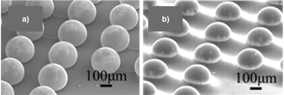
Bump absorbability and bump penetrability are the key factors for the BSF process. Bump absorbability is the ability to perform lamination without forming bubbles around bumps after heat curing.
Meanwhile, bump penetrability is the ability to perform lamination without leaving BSL residue on top of bumps after peeling the BG tape.
If bump absorbability or bump penetrability is not satisfactory, then problems such as bubbles around bumps and failure to achieve the designed thickness of the BSL can occur. Thus, high levels of protectiveness for bumps cannot be achieved.
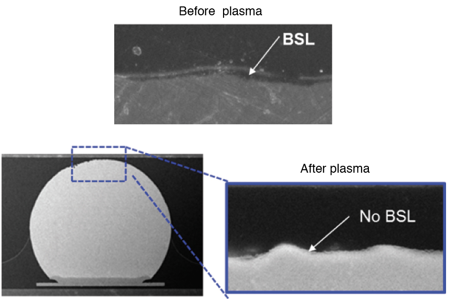
The group’s BSL is designed to increase fluidity during heat lamination (at around 70 to 90°C), and thus has good bump absorbability and penetrability (Fig. 3). Although a very small amount of BSL residue is left on top of bumps after heat curing, it has been confirmed that the residue can be removed by subsequent plasma cleaning (Fig. 4).
Reliability Tests
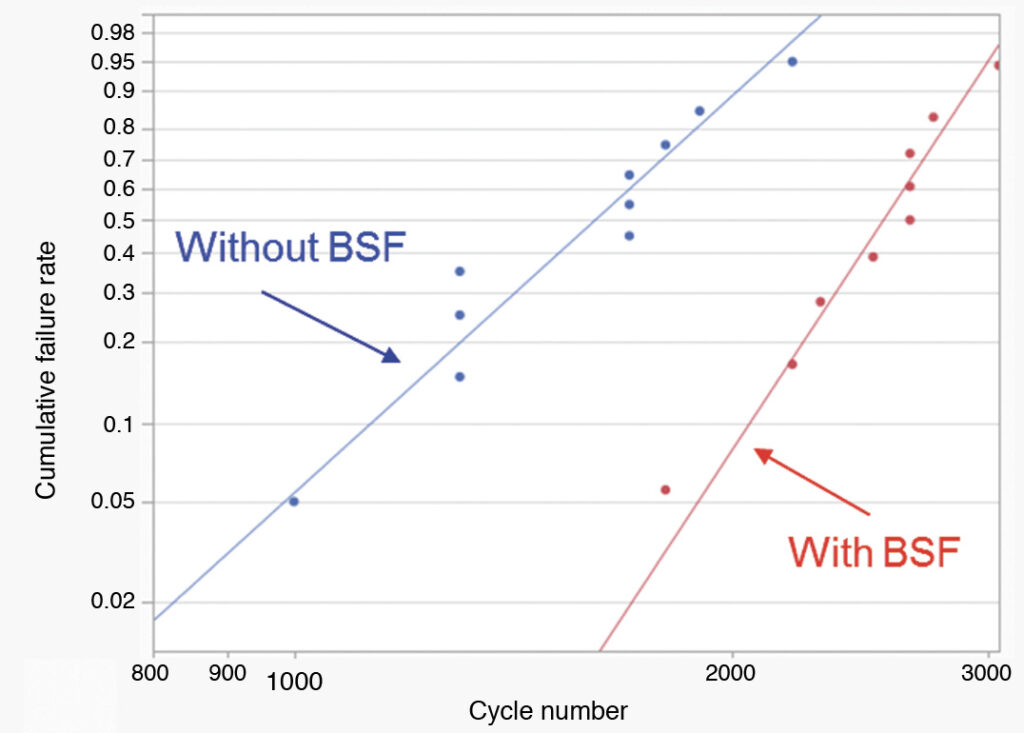
Reliability tests have been carried out to determine whether bumps were protected by BSL and whether cracks were prevented from forming on solder joints. The following chips were prepared for the reliability tests: chip thickness: 250µm; chip size: 6×6mm; bump height: 210µm; bump pitch: 400µm; and bump diameter: 250µm. Also, a BSF with a 485µm BG tape (with base material and bump absorption layer) and a 30µm BSL were prepared. The above mentioned BSF process was used to protect bump edges with the BSL. The prepared chips with the BSL were joined using joining equipment (SMT-64RH; Okuhara Electric Co., Ltd.) to a substrate where solder paste (S70G Type 5; SMIC CO., LTD.) was applied on the pad surface. Then, infrared reflow and water cleaning were performed. The reliability tests were carried out under Condition C (cycle tests lasting for five minutes each at -65°C and 150°C) for thermal cycle tests (TCT) of Joint Electron Device Engineering Council (JEDEC) Solid State Technology Association standards. For the purpose of comparison, chips to which no BSF was attached were also tested at the same time.
The results of the reliability tests are shown in Fig 5. It presents the cumulative failure rate (the proportion of chips that became defective in conduction due to crack formation on bumps) against the number of TCT cycles, using Weibull distribution. It has been confirmed that when the number of cycles was the same, the chips with the BSL had a lower cumulative failure rate than the chips with no BSL, and thus had higher reliability.
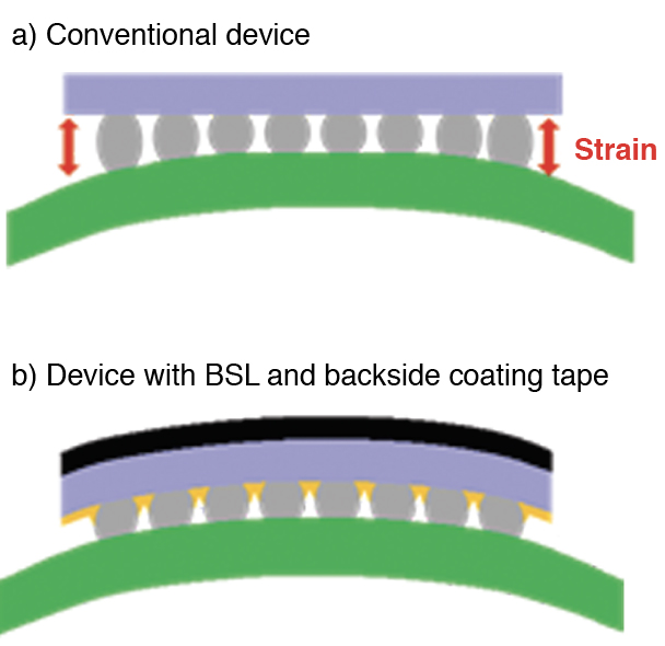
Also, it has been confirmed that reliability was further improved by backside coating tape when it was used in combination as described in the BSF process in Fig. 2. The BSL and the backside coating tape have a higher degree of thermal expansion and shrinkage than the substrates. It is believed that they relax the bending stress of substrates due to temperature changes after mounting of chips, allowing for high reliability (Fig. 6).
Conclusion
The group’s BSF has good bump absorbability and bump penetrability, and can protect bumps. It also has high reliability, so it can be considered as a material that can contribute to developing high-performance chips in WLCSP manufacturing processes.
- Share:


About This Article:
The author is, Yoichi Inao from LINTEC Advanced Technologies (Taiwan), Inc.