ASIA ELECTRONICS INDUSTRYYOUR WINDOW TO SMART MANUFACTURING
Power ICs Shape up to Meet Emerging Automobile Trends
As if the impact of novel coronavirus (COVID-19) pandemic is not enough, challenges in the manufacturing supply are becoming even more apparent beset by lingering shortage in semiconductors.
There are several reasons for the shortages. One of the major reasons is the rapid expansion in the demand for semiconductors caused by the electrification of automobiles, or the shift to electrified vehicles (xEVs). This trend is in line with the efforts to target net zero emissions of carbon dioxide (CO2). Recently, supply-demand balance of power devices has also become tight.
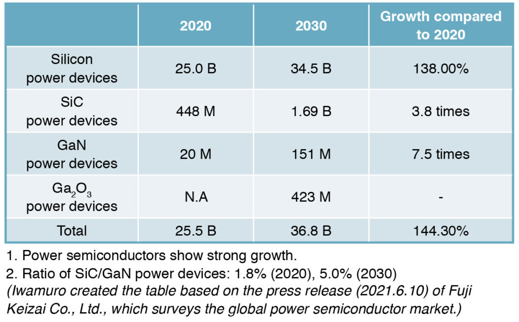
In the future, however, new opportunity for the demand expansion of power devices will come around with the rapid recovery of vehicle production, which plunged amid the COVID-19 pandemic. A recent survey conducted by a research firm revealed potentials of power devices market to expand more than 40 percent in the next 10 years (Table 1).(1)
This article introduces recent progresses of silicon devices that continue to be the main components in the power devices market, particularly silicon insulated-gate bipolar transistor (IGBT) power semiconductors. In addition, also digs deep on the latest developments of silicon carbide (SiC) and gallium nitride (GaN) power devices that attract attention as next-generation power devices, and the challenges they face.
Progress of Silicon IGBT
In xEVs, inverters for drive motors and DC/DC converters that boost battery voltage incorporate power devices. At present, 600 to 1,200V class silicon IGBT modules are mainly used. Once, IGBTs were considered to have almost reached their limits for further improvements of characteristics. However, looking at recent technological trends, development speeds have not slowed down at all.
A better surface structure has led to further improvement of the trade-off characteristics between on-state voltage drop and turn-off loss. It led to the development of IGBT module technology that guarantees maximum junction temperature (Tjmax) of 175˚C.(2) This also paved the way for mass production technology using 300mm wafers.
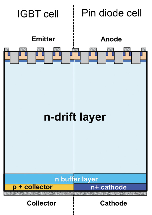
Furthermore, reverse-conducting IGBT (RC-IGBT) that integrates IGBT and pin diode (FWD) on a single chip has been developed.(3,4) In particular, RC-IGBT has undergone remarkable progress, and the application of RC-IGBT modules in xEVs has begun (Fig. 1).
SiC Power Devices
SiC has larger energy band gap (Eg) and thermal conductivity than silicon and enables the design of power modules with high Tj of 200 ˚C and higher. Thus, SiC is expected to achieve smaller and lighter cooling components.
In addition, among compound semiconductor materials, SiC is the only semiconductor material that can selectively form n-type and p-type impurity layers with a wide range of concentration through ion implantation.
Also, SiC can form silicon oxide film (SiO2) that has been used as a material for protective film for silicon semiconductors relatively easily. These characteristics enable the creation of metal-oxide semiconductor field-effect transistors (MOSFETs) using SiC.
The biggest appeal of SiC-MOSFETs for application in xEV power electronic devices is their low loss characteristics and high Tj operation, which enables smaller heat dissipation fins, and hence, the realization of smaller and lighter inverter equipment.
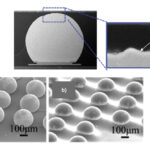
In order to aim for even lower loss, the trench MOSFET structure, which achieves finer transistor cell structure and enables lower on resistance, is expected to become the mainstream of SiC-MOSFETs (Fig. 2).(5,6)
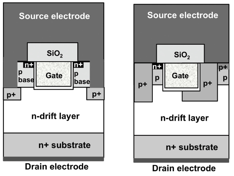
Furthermore, as lower on resistance can be achieved through the finer trench gate structure, the chip area of SiC-MOSFETs can be reduced. As a result, the number of devices that can be produced from a single SiC wafer increases. This combines with the improvement in the non-defective rate to enable the reduction of per MOSFET device cost.
The biggest challenge for wider use of SiC-MOSFETs is how to reduce cost. To achieve this, further cost reduction of SiC substrate itself is anticipated. In addition, there have been active moves to overcome this challenge making full use of mass production technology and design technology of fine trench gate structure accumulated in the 6-inch SiC Schottky barrier diodes (SiC-SBDs).
GaN Power Devices
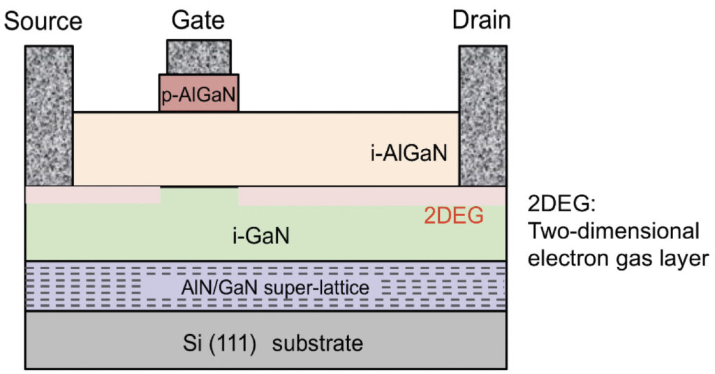
At present, main products of GaN power devices are high electron mobility transistors (HEMTs) formed on GaN on silicon substrate. GaN-HEMT devices with a lateral structure are not suitable for high-current applications. On the contrary, as they have small interelectrode capacitances, they exhibit excellent high-speed switching characteristics.
Furthermore, AlGaN/GaN-based HEMTs have strong piezo effect and spontaneous polarization effect and can form two-dimensional electron gas (2DEG) layer with high mobility and high carrier concentration on the AlGaN layer and undoped i-GaN boundary with extremely low impurity concentration.
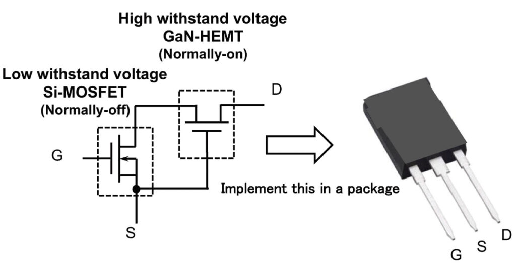
Using AlGaN/GaN-based HEMTs for conduction channels achieves low-on resistance elements, and as a result, high-efficiency and high-frequency devices can be achieved. GaN-HEMTs flow drain current with the addition of voltage between source and drain even if gate voltage is zero volt, and exhibit normally-on operation.
However, if GaN-HEMTs are to be applied to automotive power electronics devices, the achievement of normally off operation is indispensable from the viewpoint of failsafe of devices.
There are methods to achieve normally-off characteristics in a single-chip GaN-HEMTs by devising element structure. These include a structure to implement cascode-connected low withstand voltage silicon MOSFET and GaN-HEMT in a single package to make an apparent normally-off structure (Fig. 3)(7), and a gate injection transistor (GIT) structure (Fig. 4).(8)
References:
1) Fuji Keizai Co., Ltd., Press Release, https://www.fuji-keizai.co.jp/, June 10, 2021)
2) J. Kawabata et al., Fuji Electric journal, vol.88, no.4, pp.254-258, (2015).
3) K. Satoh et al., in Proc. PCIM Europe, pp.73-78, May, (2006).
4) M. Takahashi et al., in Proc. PCIM Europe., pp.438–444, May, (2016).
5) T. Nakamura et al., in IEEE IEDM Tech. Dig., pp.599-601, Dec., (2011).
6) D. Peters et al., in Proc. ISPSD 2017, pp.239–242, May, (2017).
7) T. Kikkawa et al., in IEEE IEDM Tech., Dig., 2.6.1, pp.40-43, (2014).
8) Y. Uemoto et al.,”IEEE Trans. Electron Devices, vol. 54, pp.3393-3399, (2007).
- Share:


About This Article:
The author, Noriyuki Iwamuro, is Professor at the Faculty of Pure and Applied Sciences, University of Tsukuba, Japan.