ASIA ELECTRONICS INDUSTRYYOUR WINDOW TO SMART MANUFACTURING
Inkjet-Based OLED Technology to Simplify Fabrication
The online edition of Display Week 2021, organized by the Society for Information Display (SID), was held from May 17 to 21. At the show’s 58th edition, participants from around the world recognized new technological advancements in organic light-emitting diode (OLED), micro LED, and augmented reality (AR)/virtual reality (VR), as well as in electronic paper, and digital signage. The online event allows visitors to view
firsthand advancements in AR and mixed reality (MR), printed display, auto tech, electronic paper, digital signage, and wearable technologies.
This year’s symposium features 69 technical sessions comprising 282 oral presentations, 98 of which were invited presentations; and 115 poster presentations. There were 119 presentations from China, 70 presentations from the United States, and 65 presentations from Korea. Presentations from Japan have been declining over the past years. In the past, the event has been attracting more than 10,000 participants.
This article series will feature presentations that captured the attention of the author and will be divided into two parts. Specifically, Part 1 introduces a presentation by Konica Minolta, Inc. titled “New Conceptual OLED Based on Highly Simplified Architecture and Fabrication Method.”
Fabrication Methods of OLEDs
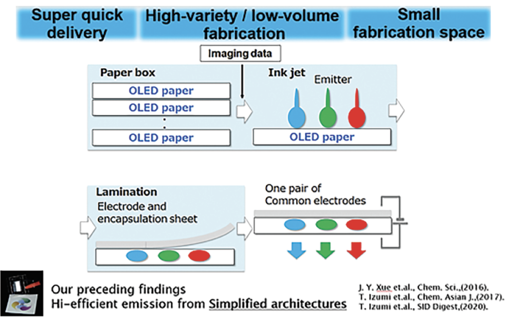
Recently, an on-demand device manufacturing method has been developed using inkjet technology. The technology is expected to significantly simplify the fabrication of OLEDs by applying smart printing to the lighting field, eliminating the need to depend on specialized plants. Among the advantages of this technology include short delivery time; enables high-variety, low-volume fabrication; and can be fabricated in a small space, thus providing opportunities for the opening of new businesses.
Fig. 1 shows the fabrication concept of the developed simple OLEDs. This method is based on the findings that high-efficient emission can be achieved using simplified OLED architectures. Using the simplified architecture enables fabrication of various images through inkjet printing on prepared OLED paper without using the bank structure. Fabrication can be completed easily by laminating the electrode and the encapsulation sheet.
Experiments
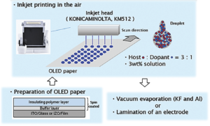
Fig. 2 shows the fabrication process of simple OLEDs, which was developed by Konica Minolta. Insulating polymer layer, which functions as an ink absorbing layer, was spin-coated on the buffer layer. Next, the inkjet process was conducted in the air using a 3wt% ink solution, a mixture of host and dopant in the ratio of 75:25. The inkjet head used was KONICAMINOLTA, KM512 with 512 nozzles, a resolution of 360dots/inch, minimum volume of each droplet of 4pL, and print dot pitch of 140μm. Following the inkjet printing, the OLED paper was dried in the air at room temperature, and potassium fluoride (KF) and aluminum (Al) were evaporated in the vacuum, thus, achieving simple OLEDs.
Results and Discussions
Simple OLEDs
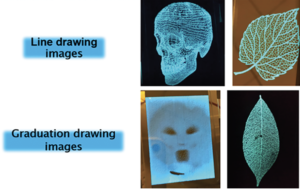
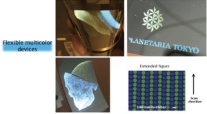
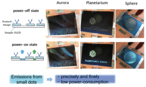
Konica Minolta has fabricated several types of simple OLEDs. The architecture of simple OLEDs consists of insulating polymer layer, KF layer and Al layer with anode, buffer layer, and host and dopant dots. Figs. 3 and 4 show single color devices and flexible multicolor devices, respectively. The light emission region consists of an assembly of dots with a diameter of about 100μm. Dots are arranged in parallel in multicolor devices (Fig. 5).
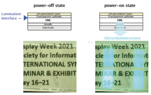
Transparent electrode laminated OLED
The fabrication process started with the spin coating of the light emission layer using 1wt% solution of the mixture of host, dopant and polymer at the ratio of 38:12:50. Next, indium tin oxide (ITO) was deposited on the polyethylene terephthalate (PET) membrane as a transparent cathode sheet using the spattering method. Finally, the film was laminated with a pressure of about 0.1Mpa at heating temperature of 363K. With the application of input voltage of 10V, bright electroluminescence (EL) was obtained as shown in Fig. 6.
Conclusions
Konica Minolta reported a new conceptual OLED technology, which adds original functions to its new lighting smart printing business. The company demonstrated a transparent electrode laminated device. In the near future, these unique technologies will likely stimulate further research on new OLED fabrication methods from the viewpoint of super quick delivery for high-variety, low-volume fabrication.
Konica Minolta has developed and demonstrated OLED devices leveraging its accumulated technologies, new device structure and fabrication process. The technologies introduced in this article are highly likely to realize a new on-demand OLED market, and future development of the technologies can be anticipated.
Reference:
T. Izumi, et all., SID2021 Digest pp.297-300 (2021).
- Share:


About This Article:
The author, Yasuhiro Ukai, Ph.D., is from Ukai Display Device Institute (UDDI).