ASIA ELECTRONICS INDUSTRYYOUR WINDOW TO SMART MANUFACTURING
Japan Digs Deep in Advanced IC Manufacturing
Amid challenges facing semiconductor supply chain, Japan has expressed interest to regain its presence in the global semiconductor map and embark on advanced manufacturing and process technologies.
Various government and private organizations have already collaborated to kick-start the project. These include the Ministry of Economy, Trade, and Industry (METI), the New Energy and Industrial Technology Development Organization (NEDO), the National Institute of Advanced Industrial Science and Technology (AIST).
Tsukuba as Core
At present, Japan does not have manufacturing lines for advanced logic devices and has significantly decreased its presence in the global semiconductor market for the last 30 years. Without a doubt, the importance of semiconductors has been ever-increasing, and major countries have been strengthening their production bases.
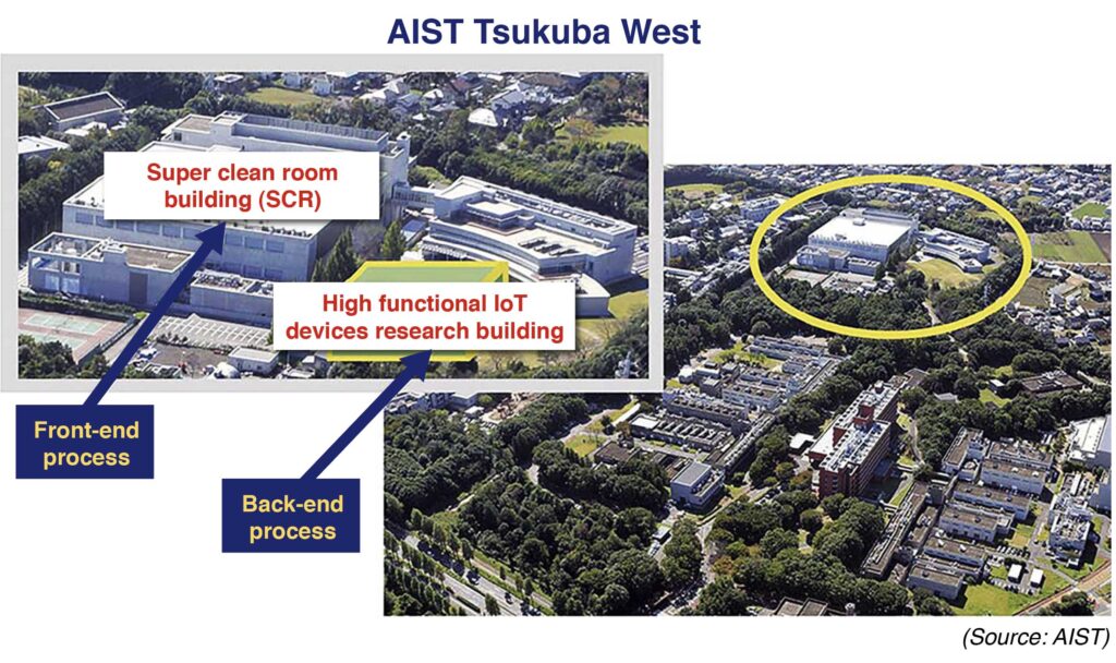
As such, Japan intends to recover from this setback by launching a government-led project. Using AIST Tsukuba West as a hub, private companies, research institutions, universities and overseas semiconductor companies collaborate to develop technologies for the front-end and back-end processes. Particularly, these processes are indispensable for the manufacture of advanced semiconductors.
The stakeholders held a kick-off event in late October and presented the outline as well as the roadmap of the project.
The project on the front-end process targets the establishment of new manufacturing and process technologies. Correspondingly, these are necessary for the creation of logic semiconductors (nanosheet transistors) with three-dimensional (3D) channel structures in the most advanced 2nm node and beyond.
Constructs Common Pilot Line
With AIST taking the key role, major semiconductor players in Japan, including Tokyo Electron Device LTD. (TED), SCREEN Semiconductor Solutions Co., Ltd., and Canon, Inc., are taking part in the project. Particularly, these three companies will leverage respective core technologies to develop advanced semiconductor manufacturing equipment. This will lead to the construction of a common pilot line to fabricate prototype nanosheet field effect transistors (FETs) in the super clean room (SCR) of AIST Tsukuba West.
To begin, TED will develop next-generation manufacturing equipment and new materials beyond next-generation materials. Meanwhile, SCREEN will develop advanced cleaning technology and next generation annealing technology. On the other hand, Cannon will develop nanoimprint lithography technology.
Moreover, the companies will exchange wafers with the pilot line to verify them in the nanosheet structure. This in turn will lead to establish manufacturing technology.
At present, 5nm is the most advanced microfabrication technology on the commercial base. Taiwan Semiconductor Manufacturing Company Limited (TSMC) and Samsung Electronics Co., Ltd. target mass production in the 2nm node and beyond around 2024 to 2025.
AIST explained, “IC transistors of the 2nm node will undergo paradigm shift from FinFET to Nanosheet FET. This has a very complex structure, and it is difficult for a single company to develop and validate manufacturing technology. The three companies each develop leading-edge equipment for Japan to have manufacturing process technology.”
At present, 65nm CMOS line is in operation in the SCR, and the installation of 20 new equipment is in the pipeline already. Four technologies: fine lithography technology, nanosheet structure formation technology, gate stack formation technology, and nanosheet transistor integration technology will rise in the front-end project.
Japan-Led Consortium
In the most advanced manufacturing sites, the use of extreme ultraviolet (EUV) lithography equipment has been expanding. However, the pilot line does not install EUV equipment, and the use electron beam direct drawing equipment for processes that require EUV.
AIST sets up a consortium to enable companies and universities working on research and development of advanced semiconductors, as well as the three companies, including TED, to use the common pilot line. In addition, five semiconductor companies, including TSMC, Intel and IBM, will also participate.
The installation of equipment in the line will start in Feb. to Mar. 2022 and the new equipment will start rolling in late 2022. Furthermore, nanosheet FET full process will become available in FY2025.
The post-end of the project will aim for higher integration and performance for the 3D packaging technology. TSMC Japan 3DIC Research and Development Center, a Japanese subsidiary of TSMC, will lead the project.
The development base will emerge in the high-functional internet of things (IoT) devices research building adjacent to the SCR building of AIST. At present, TSMC is constructing the line. Operation of the line and research and development will commence by the end of FY2022.
- Share: