ASIA ELECTRONICS INDUSTRYYOUR WINDOW TO SMART MANUFACTURING
Race for global foundry chip markets heats up
Race for global foundry chip markets heats up
By KDJ
Seoul (2021/08/06)- All of a sudden, the global foundry chip making market is in a state of flux, as newcomer Intel Corp. is coming out of nowhere to join the fray to seize control of the US$80.5 billion-a-year-market.
Market leader TSMC is now going on a spending spree to further consolidate its leadership in scale and technology.
Distant No.2 Samsung Electronics is trying to catch up with formidable market leader TSMC, counting down the time scale to 2030, the year that the Korean chip maker set as a watershed momentum for topping the list of global foundry chip makers.
5 months after it declared its re-entry into the foundry chip market in March, microprocessor chip giant Intel is now revving up its money machine to buy out global No.3 foundry chip maker GlobalFoundries.
Intel is reported to stage a tug-of- war with GlobalFoundries to reach a buy-out deal – a move to buy a much-needed scale to guarantee a success in the high-stake market.
Back in March, Intel announced that the chip maker would earmark US$20 billion for its war chest to finance its advances into the foundry business, turning up heat in the head-on race to conquer the worldwide foundry chip market.
Headquartered in New York, GlobalFoundries is the world’s third largest foundry contract chip maker that runs fab facilities in the U.S, Singapore and Germany, serving fabless chip makers like Broadcom, AMD, and Qualcomm.
At stake is the highly-prized global foundry chip making market which Intel CEO Patrick Gelsinger predicted would reach US$100 billion by 2025.
Turn Up Heat
The foundry chip business is a sort of contract chip fabrication that produces no chip of its own design, but just churn out chips of other customers’ design, who are called as fabless chip makers
As a wealth of new applications like IoT, AI, smart factories and smart cities, EVs, and autonomous driving, demand for various chips are exploding. So is that for chip making capacity, opening up new market opportunities for foundry chip makers.
Current chip shortages are the convincing illustrations of how deep global chip making capacity is running short of demand, as fabless chip makers are clamoring for more of chip fabrication capacities to address explosive demand for chips from CPUs to GPUs to mixed signal and analog chips.
Market research firm Gartner has recently predicted that global foundry chip market would grow from US$80.5 billion in 2020 to US$94 billion in 2022.
What matters the most in the race for the high prize are scale and technology.
For example, market leader TSMC has an ambitious and outlandish plan to build its brand new 300mm wafer fabrication facilities in Arizona, U.S. and Japan to serve fabless chip makers there.
That’s part of TSMC’s ambitious plan to invest US$110 billion over the next 3 years to build new fab facilities.
Intel is also working on its plan to build two brand new foundry chip making facilities in Arizona, U.S. to serve U.S. fabless chips makers. Intel is known to sign contract chip-making deals with Amazon and Qualcomm to produce chips of the two companies’ design starting from 2024. On top of that, Intel said that it has been negotiating with about 100 fabless chip makers to persuade them to outsource their chip fabrication to its brand new chip facilities in Arizona.
Scale and Technology Matters
Samsung is ambitious, too, as the world’s largest memory chip maker already declared its strong intention to invest more than US$133 billion through 2030 to outgrow TSMC in scale.
As part of the ambition, Samsung announced in late May that it would invest US$17 billion in Austin Texas, a hub to Samsung’s U.S. wafer fab operation. Back home, the chip maker also plans to invest to build one more foundry fab line in its Pyeongtaek wafer fabrication cluster.
Scale is one of the two keys to winning in the competition, as it allows foundry chip makers to produce more of chips at a relatively lower cost.
As important is technology, as it not only enables them to get more of chips out of silicon wafer, but also fabricate faster, smaller but power-thriftier chips.
Leading the race for a technology migration to finer design rules – the measure of how thinly the chip circuitry is scaled down- are TSMC and Samsung Electronics.
The two arch-rivals are the only two that can fabricate chips of 5 nanometer circuitry in high volumes.
At issue is now when and who will ramp up to a 3 nano circuitry technology earlier than competition.
TSMC is expected to start volume production of its 3 nanometer circuitry chips in the second half of 2022 using a FinFET transistor technology.
TSMC has already been testing the technology with its customers. Compared with its 5nanometer node technology, the 3nanometer node chip design rule will allow chips of that circuitry to perform better by a factor of 10% to 15%, while reducing power consumption by 25% to 30%. The transistor density will also increase by a factor of 1.1-1.7 times depending on chip structures.
Racing Down To 3nm
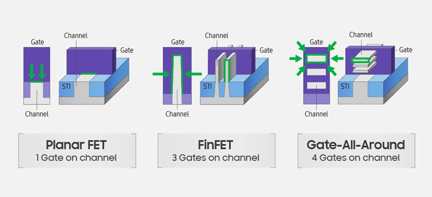
Samsung Electronics is now also working on its own GAA (gate all around)-structured 3 nanometer technology, aiming to start volume production in the second half of 2022. The GAA is a sort of multiple gate transistor technology that surround a transistor channel with multiple gates. Samsung’s GAA chip structure is made of 4 gates. Samsung is also working on MBCFET, or multu-bridge channel field effect transistor technology.
The chip maker is now fabricating 5 nanometer and 4 nanometer circuitry chips in high volume at its Pyeongtaek wafer fab fabrication cluster.
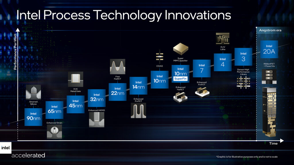
Although Intel lagged behind TSMC and Samsung in the migration to 7 nanometer circuitry technology, the PC CPU titan has an ambitious plan to ramp up to a 1.8 nanometer circuitry technology by 2025, the year that it sets as an inflection point to surpass TSMC and Samsung as a chip scaling technology leader.
Its roadmap shows that the chip maker will start mass-production of 7nanometer circuitry chips in 2022, and then ramp up to 3 nanometer circuitry technology in 2023 and 2 nanometer circuitry design rule in 2024.
Coming finally is a near-atom size 1.8 nanometer chip processing technology.
On the road toward that final destination, Intel will start implement two brand new chip structure technologies in its 2nanometer technology called 20A node
The two innovations are RibbonFET, Intel’s own version of GAAFET (gate all round field effect transistor), and PowerVia
The GAAFET is to wrap around channels with multi transistor gates on all sides to have better electrical control over channel allowing it to suppress off-state current leakage. Multiple gates also offer better drive current in the on-state as well as better analog performance, helping cut power consumption and improve performances.
The second innovation PowerVia is a backside power delivery network where all power delivery systems are removed from the top interconnect layer. Instead, they are moved to the bottom layer to be directly connected to the transistor without going through the interconnect stack. This technology also helps cut power budgets
- Share: