ASIA ELECTRONICS INDUSTRYYOUR WINDOW TO SMART MANUFACTURING
HORIBA Develops New Thin-Film Inspection System
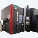
HORIBA STEC, Co., Ltd. has released the “Xtrology” fully automated thin-film inspection system.
In recent years, the number of inspection items in the manufacturing process has increased. Mainly, this is due to technological advances in the semiconductor industry. Also, the level of inspection requirements continues to rise.
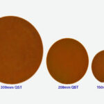
Particularly, the new product, “Xtrology,” is a highly customizable system that allows manufacturers to select one or multiple sensors from three analysis methods; these are spectroscopic ellipsometry*1, Raman spectroscopy*2, and photoluminescence*3. Accordingly, this has made it possible to perform important inspections, such as film thickness measurement, defect analysis, and composition analysis of various wafers with a single instrument.
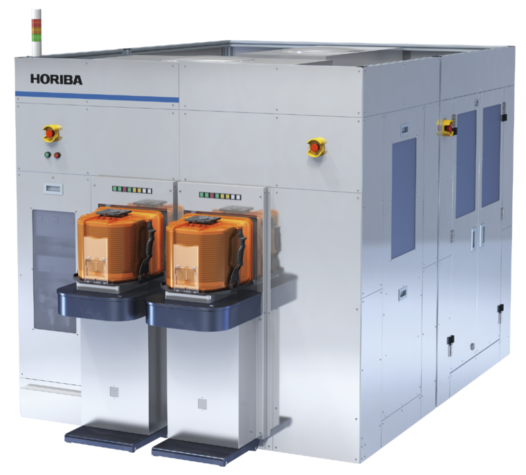
Aside from an automation function, which combines HORIBA’s in-house developed automatic conveyance system and non-destructive, non-contact sensors, the new inspection system also connects multiple external devices, such as open cassettes, SMIF (Standard Mechanical Interface), and FOUP (Front Opening Unified Pod). Continuous measurements can be performed, contributing to more efficient inspection processes and higher yields.
Additionally, because HORIBA has developed all of the sensors, automation technology, and software installed in this device in-house, it can provide consistent services and maintenance.
Having 29 countries and regions around the world in operations, HORIBA provides long-term global support. HORIBA will continue to work on further functional enhancements, such as adding more sensors that can be installed. Also, it will respond to the diverse needs of semiconductor thin film inspection with flexible customization.
Metrology Product Line Manager Kosuke Matsumoto explains, “We developed the Xtrology as a product that conducts the inspection and defect reviews on a wide range of wafer sizes and materials used in legacy and cutting-edge processes for silicon and compound semiconductor-based devices. We offer a variety of solutions by integrating a variety of sensors and automation technologies developed independently based on HORIBA’s core technology into one platform.”
-21 October 2024-
- Share: