ASIA ELECTRONICS INDUSTRYYOUR WINDOW TO SMART MANUFACTURING
New Canon i-Line Stepper Caters to Small Wafers
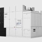
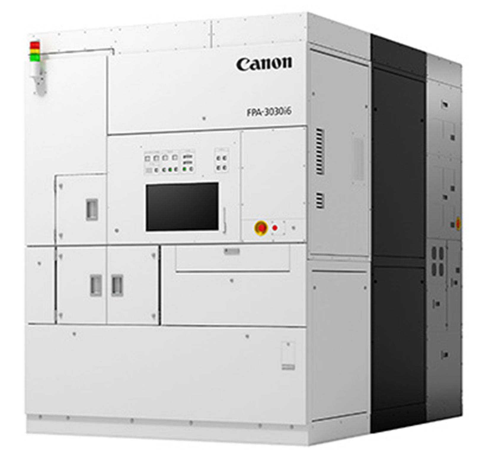
Canon Inc. releases the FPA-3030i6 i-line1 stepper, a new semiconductor lithography system for processing wafers with a diameter of 8 inches (200mm) or smaller.
Primarily, the FPA-3030i6 employs a newly developed projection lens that boasts high transmittance and high durability. The system reduces lens aberration for high-exposure dose processes and improves productivity by shortening exposure time.
Meanwhile, the lens is made of high-transmittance glass material. Specifically, it reduces lens aberrations occurring during exposure by more than 50%2 when compared to previous stepper models3. Higher transmittance also helps reduce exposure time while maintaining pattern fidelity, even under high exposure dose conditions.
Further, improving lens transmittance will also increase exposure intensity and shorten the exposure time required for each process. The FPA-3030i6 standard productivity for 8-inch (200mm) wafers has increased4 to 130 wafers per hour from 123 for the previous stepper models.
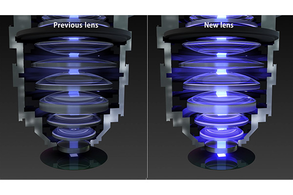
Additionally, since the lens is highly durable, the decrease of lens transmittance over time is reduced. Moreover, productivity can be maintained over the life of the system.
The numerical aperture (NA) range has also been expanded from 0.45~0.63 in the previous model to 0.30~0.63. Accordingly, this allows for a smaller NA, enabling customers to select the optimum NA for each device layer.
Optional products including a wafer handling system for special substrates are available for order to meet users’ manufacturing needs for various emerging semiconductor devices including high-power and high-efficiency green devices.
Mainly, the FPA-3030i6 suits a wider range of device fabrication thanks to a variety of available process options for silicon (Si) as well as sapphire and compound semiconductor materials, such as silicon carbide (SiC), gallium nitride (GaN) and gallium arsenide (GaAs) substrates.
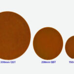
Further, Canon will offer wafer feeding options enabling handling of substrates from 2 inches (50mm) to 8 inches (200mm) in diameter, as well as thick, thin and warped substrate handling.
1 Semiconductor lithography equipment using i-line (Mercury lamp, wavelength 365 nm) light source
2 Under Canon’s standard exposure conditions
3 FPA-3030i5a (released in March 2021)
4 8-inch (200mm) wafer
-24 September 2024-
- Share: