ASIA ELECTRONICS INDUSTRYYOUR WINDOW TO SMART MANUFACTURING
Lasertec Boosts SiC Wafer Inspection with New System
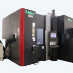
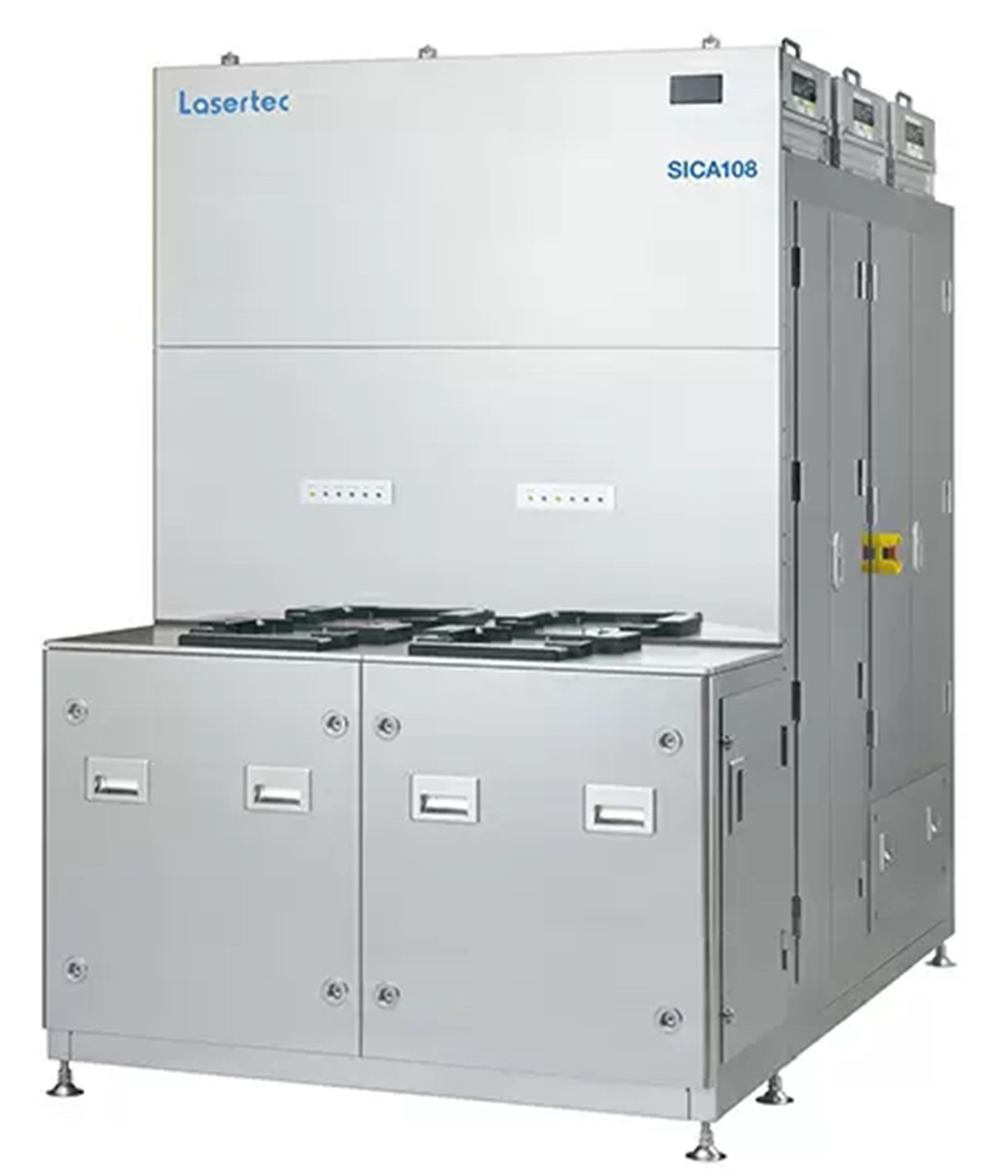
Lasertec Corporation has announced the release of SICA108, the latest model of its SiC wafer inspection and review systems. Specifically, SICA108 features both surface and photoluminescence (PL) inspection capabilities in one body. Thus, it enables customers to concurrently perform high-speed inspection and high-accuracy classification of surface defects as well as crystallographic defects.
Offers Higher Throughput, Improved Performance
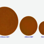
Mainly, SiC power devices are used in a variety of applications, including electric vehicles, air conditioners, solar cells, and railway cars. More importantly, they facilitate the realization of a carbon-neutral society. However, SiC wafer production processes are technically demanding, and there are still many defects that impact device yields. Therefore, it remains a challenge to manufacture high-quality SiC wafers stably at a lower cost.
In this regard, Lasertec has released SICA108 to help overcome this challenge. Renewing the inspection optics from SICA88, the current de facto standard tool widely used among many customers, SICA108 provides higher throughput and improved performance in quality analysis of SiC wafers with a lower cost of ownership.
Like its predecessor, SICA108 performs surface inspection for detecting scratches, crystal defects, and particles on the wafer surface. Also, it conducts PL inspection for detecting basal plane dislocations (BPD) inside Epi layers and stacking faults (SF), concurrently and with high sensitivity. Additionally, it features a high-accuracy defect classification capability based on Lasertec’s proprietary deep learning algorithm to enable the early detection and analysis of killer defects. Moreover, it is also compatible with various automation systems used in smart fabs, such as automatic guided vehicles (AGV) and overhead hoist transports (OHT).
Lasertec will continue to pursue the development of defect inspection technologies to address customer needs and contribute to the improvement of power device quality and productivity.
Features
- Concurrent inspection of surface defects and BPD/SF at high speed and with high sensitivity
- Detailed classification of various defect types using high-accuracy Automatic Defect Classification (ADC) and high-resolution review images
- Compatible with various automation systems, including AGV and OHT
Applications
- Incoming and outgoing inspection of SiC bare wafers and SiC Epi wafers
- Monitoring of SiC epitaxial growth processes
- Monitoring of SiC polishing processes
- Management of SiC device manufacturing processes
-25 September 2024-
- Share: