ASIA ELECTRONICS INDUSTRYYOUR WINDOW TO SMART MANUFACTURING
OKI Tech to Surge New Ultracompact Photonic IC
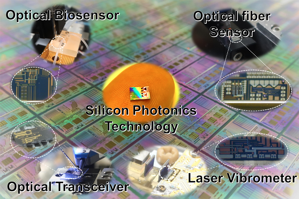
Using silicon photonics technology for semiconductor optical circuits, OKI has successfully developed an ultracompact photonic integrated circuit chip. Specifically, with a broad range of potential applications, including optical fiber sensors, laser vibrometers, and optical biosensors.
This makes it possible to achieve ultra-miniaturization and low power consumption similar to LSI (Note 1). Moreover, it will also dramatically lower costs through mass production of optical sensor modules. Optical sensors are a technology that uses optical fibers and optical waveguides with low light loss. Particularly, they can detect, process, and transmit physical phenomena such as vibration, strain, and temperature in the form of light. Furthermore, they are themselves a green technology that realizes sensing while saving energy.

Silicon photonics technology is a technology that can broaden the scope of applications for optical sensors previously limited to localized use. Also, it also can make a significant contribution to the advancement of GX (Note 2).
Bears Fruit of R&D
To address various issues faced by modern society, this requires high-precision sensor technology and network technology. Specifically, capable of seamlessly collecting vast amounts of sensor data. While high-precision optical sensors that take advantage of the property of light, that is, low energy loss, are one effective technology to realize the above. Accordingly, their large size and high cost have limited their applications to a few areas such as research and large-scale infrastructures.
OKI has engaged in research and development on silicon photonics technology over many years. They need to enter on optical transceivers, with the scope of this research still currently expanding to include various optical sensors. Moreover, silicon photonics technology is a technology that integrates complex optical circuits—previously realized by wiring individual optical components with optical fibers—on a silicon substrate using semiconductor microfabrication technology.
It makes use of the same manufacturing methods as LSI, which is vital for computers, enabling miniaturization, energy saving, and cost reduction through mass production. Devices that were previously large, heavy, and cumbersome can now be downsized to dimensions comparable to a smartphone or tablet, greatly expanding the scope of optical sensor applications.
In November 2023, OKI announced its technology strategy through to 2031. The Edge Platform is a technology concept to expand the value provided through edge advancement and data connection and linkage based on OKI’s core competence of “robustness,” which has supported social infrastructures.
Moreover, the technology strategy includes bolstering optical sensing technology across a wide range of areas, from social infrastructure monitoring to the medical field. The development of this photonic integrated circuit chip is based on this technology strategy and is the result of fully capitalizing on silicon photonics technology.
Example applications
The chip can be applied to the following uses:
• Optical fiber sensors
The miniaturization and cost reduction achieved by optical integration allow the scope of applications to expand to the monitoring and maintenance of broad-ranging social infrastructures, including bridges, tunnels, and slopes.
• Laser vibrometers
The volume ratio of approximately 1/200,000 against conventional optical circuits enables mounting on drones and robots. Utilizing wider frequency characteristics than general vibrometers contributes to more sophisticated equipment inspections and labor saving.
• Optical biosensors
Optical biosensors are capable of quickly and easily distinguishing between multiple, disparate biomaterials, contributing to the advancement of testing in the fields of biotechnology and healthcare.
• Optical transceivers
Optical transceivers enable the production of ultracompact, low-cost, high-speed transceivers for optical access networks, contributing to large-capacity data communications.
Terminology
Note 1: LSI (Large-scale integration)
Device that densely integrates microscopic electronic components and wiring on a semiconductor chip such as silicon
Note 2: GX (Green transformation)
Initiatives aimed at reducing greenhouse gas emissions to achieve a sustainable society
14 November 2024


