ASIA ELECTRONICS INDUSTRYYOUR WINDOW TO SMART MANUFACTURING
Imec’s New 300mm GAN Track to Soar Novel Power Devices
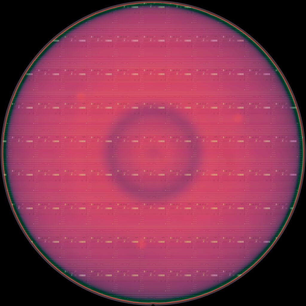
Nanoelectronics research and innovation hub imec has introduced a new program track centered on 300mm gallium-nitride (GaN) open innovation track for low- and high-voltage power electronics applications.
Moreover, it has welcomed leading companies such as AIXTRON, GlobalFoundries, KLA Corporation, Synopsys, and Veeco as first partners for the said track.
The program track aims to develop 300mm GaN epi growth, and low and high voltage GaN high electron mobility transistor (HEMT) process flows. Therefore, this will pave the way for the transitioning to 300mm wafer sizes.
The use of 300mm substrates will not only reduce GaN device manufacturing costs, but it will also allow the development of more advanced power electronics devices, such as efficient low-voltage point-of-load converters for CPUs and GPUs.
Trends Toward GaN Technology
Recently, the market has seen the introduction of GaN-based fast battery chargers, which underscores the potential of GaN technology for power electronics applications.
GaN technology is poised to enable a new generation of power electronics products. In fact, there has been continuing progress made in GaN epi growth, GaN device and IC manufacturing, reliability and robustness, and system-level optimization. These will enter the market with reduced form factors, smaller weight, and superior energy conversion efficiency compared to Si-based solutions.
Examples of these are on-board chargers and DC/DC converters for automotive applications, inverters for solar panels, and power distribution systems for telecom and AI data centers. These are the fields where GaN-based building blocks contribute to the overall decarbonization, electrification and digitalization of society.
A notable trend in GaN technology development is the move to larger wafer diameters, with capacity now mostly available on 200mm. With the launch of its 300mm GaN program track, imec is taking the next step, building on its 200mm expertise.
Stefaan Decoutere, fellow and program director of the GaN power electronics program at imec: “The benefits of transitioning to 300mm wafers go beyond upscaling production and reducing manufacturing costs. Our CMOS-compatible GaN technology now has access to 300mm state-of-the-art equipment that will allow us to develop more advanced GaN-based power devices. Examples are aggressively scaled low-voltage p-GaN gate HEMTs for use in point-of-load converters, supporting energy-efficient power distribution for CPUs and GPUs.”
Robust Ecosystem
The launch of the 300mm GaN program follows successful 300mm wafer handling tests and mask set development. Imec expects to have full 300mm capabilities installed in its 300mm cleanroom by the end of 2025.
“The success of the 300mm GaN development also hinges on the ability to establish a robust ecosystem and jointly drive innovation from 300mm GaN growth and process integration to packaging solutions,” adds Stefaan Decoutere. Aside from AIXTRON, GlobalFoundries, KLA Corporation, Synopsys, and Veeco, imec expects to welcome more partners soon.
06 October 2025
- Share: