



ASIA ELECTRONICS INDUSTRYYOUR WINDOW TO SMART MANUFACTURING
ASMPT Powers India Across Full Packaging Spectrum
India’s semiconductor manufacturing sector is scaling up rapidly, and ASMPT is backing the country’s full packaging journey. Addressing this industrial shift, Benedict Yuen, Regional General Manager, Rest of Asia, ASMPT, emphasized in an interview with AEI that the company supports local manufacturers from high-volume mainstream assembly today to advanced packaging as the ecosystem matures.
Full Spectrum Strategy Anchors Indian Chip Packaging
“ASMPT supports customers across the full packaging spectrum, from mainstream assembly and test today through to advanced packaging as the ecosystem matures,” Yuen said at SEMICON India 2026. High-volume processes—including die bonding, wire bonding, flip chip, molding, and test handling—form the immediate foundation of India’s assembly, testing, marking, and packaging (ATMP) capacity. “These are the processes that will define the competitiveness of India’s first wave of facilities, and they are processes ASMPT has been refining with customers for decades,” Yuen explained.
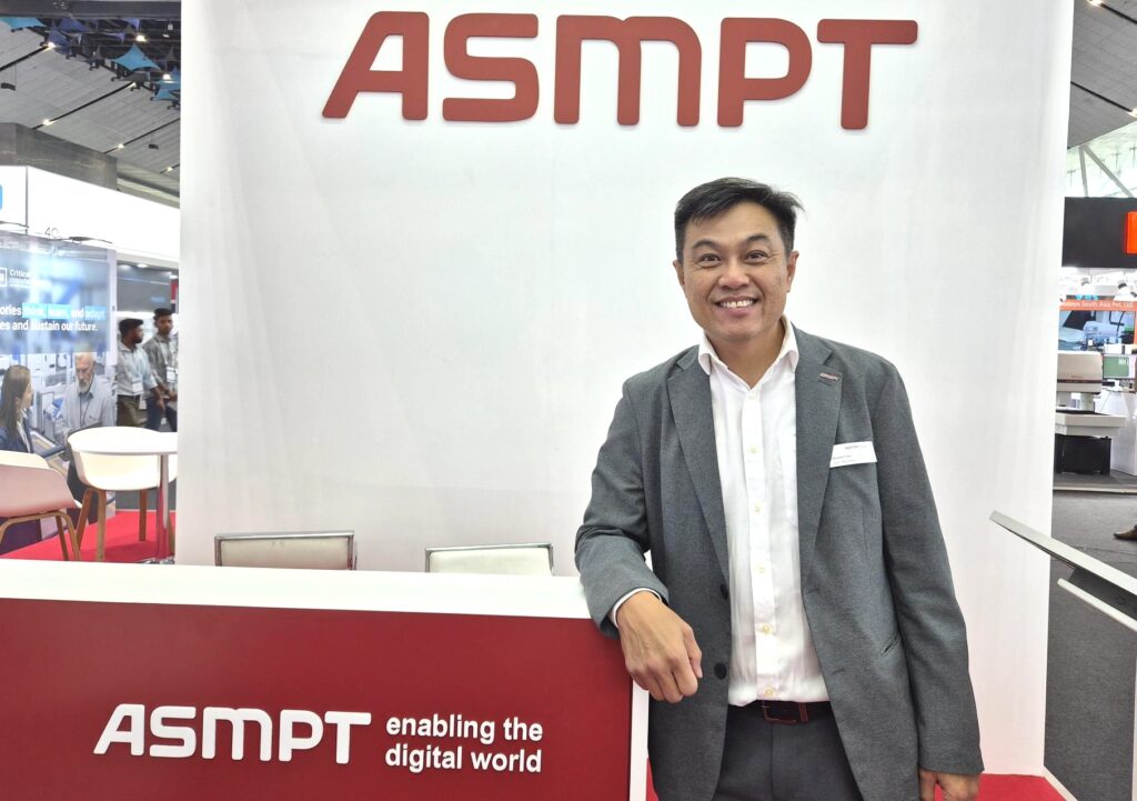
ASMPT ensures process continuity as facilities scale. Manufacturers do not need to choose between present operational demands and future technical upgrades. “As their product mix moves towards higher-value packaging, whether fan-out, thermocompression bonding or power modules, the same partner and the same process knowledge carry forward,” Yuen noted. “What we bring to India is not a prototype. It is proven technology already running in volume elsewhere,” Yuen added.
Policy Certainty Speeds Yield to Market
Government frameworks like the India Semiconductor Mission (ISM) offer strong national policy certainty. This long-term commitment allows global equipment leaders and domestic OSATs to invest confidently.
“ISM-backed ATMP and OSAT projects need to move from construction to qualified production on tight timelines, and that puts a premium on equipment with a proven track record,” Yuen said. “Speed to stable yield is the commercial test these projects face first, and it is a well-understood problem that we have solved repeatedly with customers elsewhere,” Yuen pointed out.
Automotive and EV Boom Demands Dual Capabilities
India’s expanding automotive and electric vehicle (EV) sectors require both mainstream assembly and advanced packaging running simultaneously. Mainstream packaging houses critical microcontrollers, sensors, and discrete power devices built for long life cycles and zero-defect requirements. Concurrently, EV electrification relies on silicon carbide (SiC) devices that demand advanced packaging to manage high thermal and electrical loads.
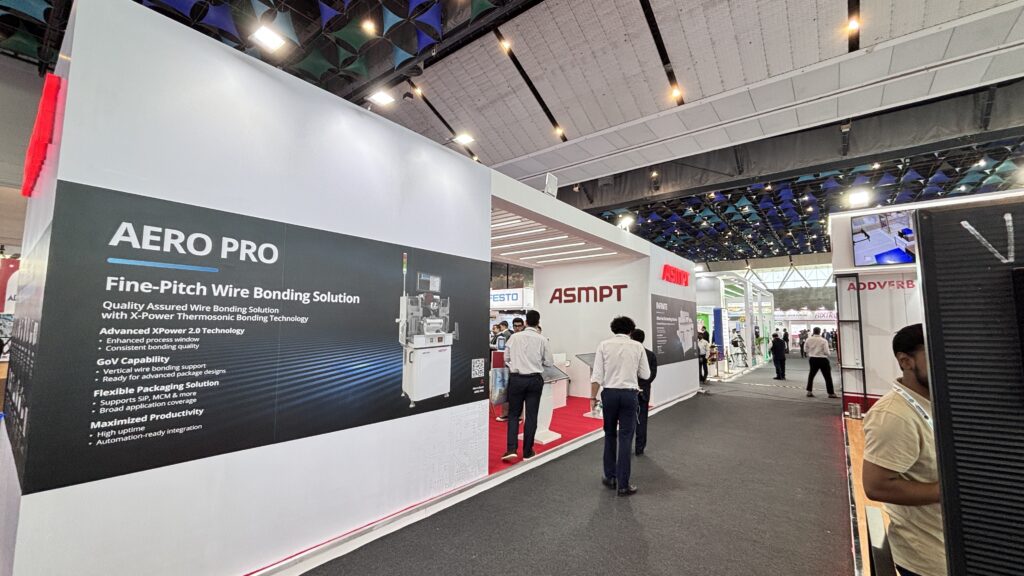
“Automotive is the clearest example of why the full packaging spectrum matters, because the sector depends on mainstream and advanced packaging running side by side,” Yuen observed. “A large share of automotive semiconductor content sits in mainstream packaging,” Yuen said, while noting that electrification adds higher thermal requirements for power modules.
Local Engineering Talent Drives Software Performance
Modern semiconductor packaging is increasingly driven by software intelligence, machine analytics, and process control. India’s deep software and data engineering talent pool gives the region a direct, structural advantage in scaling advanced manufacturing.
“Semiconductor assembly has become a software problem as much as a mechanical one,” Yuen highlighted. “India has a deep, mature software and data engineering base, and those skills transfer directly into this work,” Yuen concluded, reinforcing ASMPT’s commitment to building production-ready capacity in India.
25 September 2026
– Cristian Canoza
- Share: