


ASIA ELECTRONICS INDUSTRYYOUR WINDOW TO SMART MANUFACTURING
Silicon to Systems: India’s US$200B Chip Blueprint
In this exclusive interview, Ashok Chandak, President of IESA & SEMI India, details how the new Semicon 2.0 framework and a projected $200B market shift are positioning India as a global ecosystem leader.
India’s semiconductor trajectory is undergoing a fundamental structural shift. A landmark report by Ernst & Young (EY) India and the India Electronics & Semiconductor Association (IESA) projects the domestic chip market to surge from US$64 billion in 2026 to US$200 billion by 2035. Driven by expanding electronics assembly, AI infrastructure, electric mobility, and telecommunications, this accelerated demand reflects an underlying reality: semiconductor imports into India grew more than fivefold between FY17 ($5.7B) and FY25 ($30.3B), expanding at a 23% CAGR.
This rapid scaling builds on the momentum of the India Semiconductor Mission (ISM) 1.0. Under the initial tranche, 12 major projects representing ₹1.64 lakh crore (US$20 billion) in cumulative investments were approved—including one silicon fab, two compound semiconductor fabs, and nine packaging/assembly facilities. Significantly, five facilities have already entered commercial production and export, signaling a transition from policy declarations to operational yield.
To convert this initial footprint into global competitiveness, the Union Cabinet rolled out Semicon 2.0, backed by an enhanced outlay of ₹1,27,500 crore (US$15 billion). Rather than focusing solely on front-end fabs and back-end OSAT capacity, Semicon 2.0 targets sub-tier ecosystem depth across six pillars: indigenous design, equipment and machines, specialty chemicals and gases, advanced packaging, R&D, and specialized talent creation.
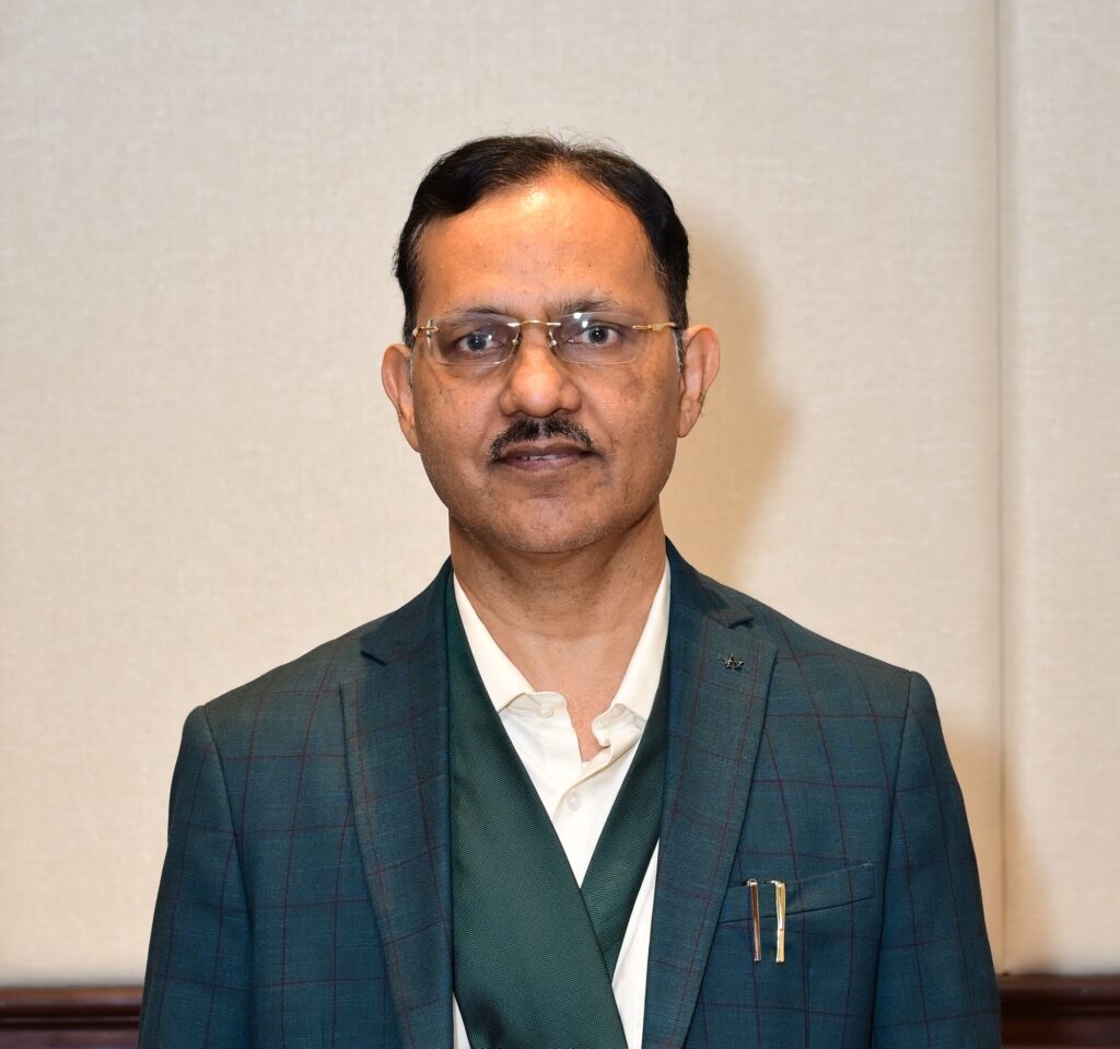
As Ashok Chandak, President of IESA and SEMI India, succinctly frames this turning point: “India has moved from credibility to capability; Semicon 2.0 is about building the ecosystem around the factories; and the ultimate opportunity is to move from Silicon to Systems.”
In this exclusive interview with AEI, Chandak breaks down what it takes to execute this US$200 billion vision, build sub-tier supply chain depth, bridge the gap between chip design and commercial manufacturing, and moving from silicon to systems.
AEI: The EY–IESA report projects India’s semiconductor market to surge to $200 billion by 2035—doubling previous target tempos. Is this growth driven by sheer hardware manufacturing volume or higher semiconductor content per device?
Ashok Chandak: It will be both, but value-per-device will become increasingly important. India is scaling massive assembly volumes across smartphones, automobiles, industrial equipment, appliances, and connected devices. But these end-products are becoming far more semiconductor-intensive.
An automobile today is effectively a computing platform on wheels. Modern industrial machines rely heavily on sensor-rich processing, while AI edge devices, smart meters, and 5G/6G telecom infrastructure require significantly greater processing power, memory, connectivity, and power management.
The opportunity is not merely to manufacture more units; it is to increase the semiconductor value embedded in every product made in India. This is why our conversation must move from Silicon to Systems. The greatest value will be created when Indian semiconductor IP, chips, advanced packaging, electronics manufacturing, and system companies work together under an integrated framework.
“The opportunity is not merely to manufacture more units; it is to increase the semiconductor value embedded in every product made in India. That is why our conversation must move from Silicon to Systems.”
— Ashok Chandak, President, IESA & SEMI India
AEI: What is the single most immediate operational risk that could bottleneck commercial production as new fabs and OSAT lines ramp up?
Ashok Chandak: If I had to identify one immediate ecosystem risk, I would point to specialized talent and supplier depth together, rather than viewing infrastructure in isolation.
India has demonstrated that it can attract capital and build large facilities. The next challenge is ensuring these facilities operate at global levels of yield, quality, reliability, and cost. That requires thousands of specialized technicians, cleanroom process engineers, equipment maintenance professionals, and supply-chain specialists.
We also need hundreds of secondary suppliers co-located around every major facility—providing specialty gases, ultra-pure chemicals, substrates, precision components, and equipment servicing. A semiconductor fab cannot operate in isolation; it requires a surrounding industrial web.
The good news is that the ecosystem is already beginning to respond. Semicon 2.0 specifically includes machines and materials and talent development, while the government has stated an objective of training one lakh technicians.
AEI: How does Semicon 2.0 explicitly address these critical secondary suppliers like gas, chemical, and equipment makers?
Ashok Chandak: That is the primary evolution under Semicon 2.0. The first phase established foundational fabs and packaging units. Phase two expands support across machines, raw materials, specialty chemicals, substrates, R&D, and workforce development.
By bringing equipment OEMs and materials suppliers into the incentive framework, global suppliers have a clear mechanism to set up local R&D and manufacturing rather than shipping inputs from overseas. We are now seeing the shift toward integrated semiconductor clusters.
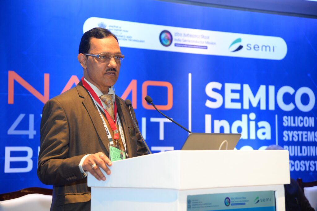
AEI: Global equipment billings reached historic highs in 2026. How is SEMI India working with major tool OEMs to anchor tool servicing and spare parts manufacturing locally?
Ashok Chandak: Equipment is one of the most strategically important opportunities within Semicon 2.0. India cannot build a resilient ecosystem if critical equipment, precision components, and servicing remain entirely dependent on foreign supply chains.
Global equipment OEMs increasingly view India as a strategic technology, R&D, and supply-chain hub. Applied Materials has announced US$5 billion investment plan through 2035—covering R&D, supply-chain localization, and workforce expansion—is a landmark example. Lam Research, Tokyo Electron (TEL), and ASML are similarly expanding their footprints.
“A semiconductor fab cannot operate in isolation—it requires a surrounding industrial web. The next challenge is ensuring these facilities operate at global levels of yield, quality, and cost.”
The immediate window for India is to build capabilities in equipment servicing, tool refurbishment, spare parts, and precision engineering, before eventually moving into sub-systems and machine manufacturing.
AEI: India houses 20% of the world’s chip design talent, but domestic startups often struggle to commercialize. How can schemes like DLI help startups move from tape-outs to high-margin volume products?
Ashok Chandak: India has proven it can design chips; the next challenge is building successful semiconductor companies. The transition must follow a disciplined path:

Government data shows over 300 chip designs developed locally, with 211 chips taped out across 75 institutions by April 2026. But financial support alone is insufficient. Startups need access to Multi-Project Wafer (MPW) runs, validation labs, packaging partners, strategic capital, and enterprise customers willing to adopt local silicon.
We must encourage domestic startups to target high-value verticals like Edge AI, automotive power electronics, smart meters, CCTV, RISC-V microcontrollers, and sensors. The objective is to build indigenous product companies, not just design-service firms.
AEI: Given global supply-chain dynamics, which specific nodes or technologies give India the strongest strategic leverage?
Ashok Chandak: Total self-sufficiency is unrealistic in semiconductors; our objective should be strategic capability and global relevance.
We should avoid an either-or approach between mature nodes and leading-edge silicon. Legacy nodes (28nm, 40nm, 65nm) and compound semiconductors (Gallium Nitride and Silicon Carbide) remain vital for high-volume automotive, industrial automation, power management, and IoT markets. Simultaneously, we must develop sub-5nm design and IP capabilities without waiting for a leading-edge fab to land locally.
The EY–IESA report highlights advanced packaging (2.5D/3D and heterogeneous integration), compound semiconductors, photonics, and chip-to-system integration as India’s highest-potential sectors. These segments allow India to combine its software and design talent with manufacturing scale to become an indispensable node in global value chains.
AEI: IESA proposed local value-addition targets of 25% by 2026 and 40% by 2030. Are these realistic for greenfield facilities?
Ashok Chandak: Localization must be pragmatic, phased, and technology-specific. A greenfield fab depends on globally qualified suppliers and certified materials; it cannot localize inputs overnight without risking yield or reliability.
We view 25% and 40% as ecosystem development benchmarks rather than blunt mandates. Local value addition must be measured progressively across raw materials, precision components, packaging, testing, software, IP, and eventually indigenous process technology. Incorporating domestic PCBs, displays, and sub-modules into the calculation builds true domestic depth without compromising global competitiveness.
“India’s semiconductor story is no longer a race to catch up. It is a journey of capability building—creating the design, manufacturing, packaging, equipment, materials, talent and systems capabilities that can make India a trusted and indispensable part of the global semiconductor value chain.”
AEI: What is your final message to global CEOs looking at India in 2026?
Ashok Chandak: My message is straightforward: India’s semiconductor story is no longer a race to catch up. It is a journey of capability building—creating the design, manufacturing, packaging, equipment, materials, talent and systems capabilities that can make India a trusted and indispensable part of the global semiconductor value chain.
Don’t look at India only as a future semiconductor market. Look at India as an emerging semiconductor capability.
The opportunity is not to replicate Taiwan, Korea or the US. The opportunity is to build an India-specific strength across design, manufacturing, packaging, equipment, materials, R&D and systems—and connect that capability to the global value chain.
India’s semiconductor journey is no longer just about announcing projects. It is about executing them, scaling them and creating the ecosystem around them.
India has moved from credibility to capability—and from Silicon to Systems.
— Cristian Canoza
25 September 2026
- Share: