
ASIA ELECTRONICS INDUSTRYYOUR WINDOW TO SMART MANUFACTURING
From Factory to Lab: IMI ATC's Vertical Quality Loop
As semiconductor devices become smaller, packaging structures more complex, and reliability requirements more demanding, advanced failure analysis is increasingly moving from a post-failure investigation function to an earlier role in product development and manufacturing qualification.
That shift is driving new investments and capability development at the Analytical Testing and Calibration Laboratory (ATC) of Integrated Micro-Electronics, Inc. (IMI), a Philippine-headquartered electronics manufacturing services (EMS) company with a global footprint.
At the recently concluded Philippine Semiconductor & Electronics Convention and Exhibition (PSECE 2026), Joey Garfin, Global Head of ATC, said advanced failure analysis is now becoming part of a broader engineering decision-making process rather than a reactive troubleshooting activity.
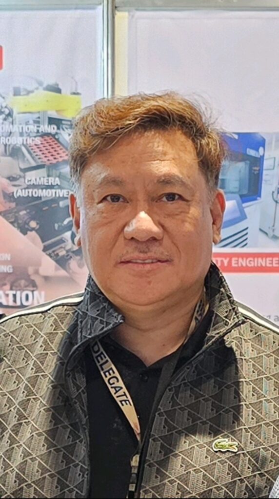
“Failure analysis used to be the corporate autopsy. But today, it is more of a product design enabler system,” Garfin said in an exclusive interview with AEI. “We are involved while materials are selected, processes are qualified, and reliability risks can still be designed out.”
The shift, Garfin added, reflects a broader industry effort to identify reliability risks earlier in the product lifecycle, helping manufacturers accelerate time-to-market, improve product reliability, lower quality-related costs, and support new product innovation.
“Failure analysis used to be the corporate autopsy. But today, it is more of a product design enabler system.” – Joey Garfin, Global Head, Analytical Testing and Calibration Laboratory
Complexity Drives New Diagnostic Requirements
According to Garfin, a combination of electrification, semiconductor miniaturization, advanced packaging technologies, and increasing product density is creating new diagnostic challenges across electronics manufacturing.
“Devices are getting smaller. Unfortunately, physics did not agree to make things simpler,” he said.
He noted that dense assemblies, thinner layers, finer interconnects, and heterogeneous material stacks require increasingly sophisticated localization, imaging, and sample-preparation techniques to identify defects accurately.
IMI’s ATC has responded by expanding capabilities in areas including advanced decapsulation, cross-sectioning, imaging, correlative analysis, and nanoscale characterization. The laboratory also invested in a Field Emission Scanning Electron Microscope (FESEM) to support nanoscale imaging and material composition analysis and is evaluating Micro-CT technology for non-destructive defect detection.
“The challenge is not merely seeing a small feature. It is exposing that feature without creating an artifact that looks like a failure,” Garfin said.
While advanced nanoscale tools handle deep root-cause investigations, everyday quality control on the factory floor often begins with rapid screening technologies like ATC’s Handheld XRF, which is one of the company’s features at PSECE 2026.
Garfin likens portable XRF to an “airport security scanner” that provides instant elemental fingerprints on the production floor, while the laboratory acts as the “forensic unit”. This tiered model allows manufacturers to catch alloy mix-ups or restricted substances on-site instantly, reserving full laboratory validation for complex or critical anomalies.
Failure Analysis Becomes a Strategic Function
Garfin said the growing complexity of electronic products means companies can no longer rely solely on end-of-line testing to identify quality issues.
Instead, advanced diagnostics increasingly influence material selection, product qualification, reliability planning, and manufacturing decisions.
“The instrument does not solve the case. The sequence of questions does,” he said, describing an investigative process that begins with non-destructive examination before progressing to more invasive analytical techniques.
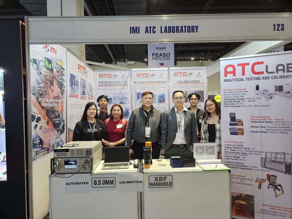
ATC currently employs a range of analytical tools, including FESEM, Energy Dispersive Spectroscopy (EDS), Fourier Transform Infrared Spectroscopy (FTIR), and reliability testing systems to support root-cause investigations and process validation.
Garfin said advanced failure analysis allows manufacturers to retain critical diagnostic work, material expertise, and reliability decision-making closer to production operations.
“High-value engineering begins when we stop treating local capability as a backup plan,” he said.
Expanding Beyond Traditional Markets
Originally established in 2006 to support IMI’s internal requirements, ATC has evolved into a commercial business unit serving both domestic and international customers. Garfin estimates laboratory utilization is split approximately equally between local and overseas clients.
Beyond serving internal manufacturing needs, ATC underwent a strategic transformation following its founding in 2006. Recognizing excess capacity, management transitioned the facility into a self-sustaining commercial business unit. Today, the laboratory maintains almost 50-50 split between local and international operations, providing rigorous testing and failure analysis to global Tier-1 automotive and technology OEMs alongside domestic clients.
“High-value engineering begins when we stop treating local capability as a backup plan.” – Garfin
While automotive and semiconductor customers remain the largest segments, the laboratory is increasingly seeing opportunities in aerospace, medical, and industrial applications. Garfin said airlines and the Philippine Space Agency have engaged with ATC on testing-related collaborations, while academic partnerships have supported medical-device development projects and engineering training initiatives.
The laboratory is also exploring how artificial intelligence can support engineering workflows through image classification, anomaly detection, spectral comparison, and analysis of historical laboratory records.
“AI will not replace analysts. But an analyst who uses AI well may replace a workflow that does not,” Garfin said.
As semiconductor manufacturing continues to advance toward smaller geometries, more complex packaging architectures, and tighter reliability requirements, the role of advanced diagnostics is likely to become increasingly important across both product development and manufacturing operations.
Cristian Canoza
04 November 2026
- Share: