ASIA ELECTRONICS INDUSTRYYOUR WINDOW TO SMART MANUFACTURING
Materials, Process Evolve with Digital Manufacturing
As the manufacturing industry upgrades to digital manufacturing, innovations flood the manufacturing processes. Specifically, laser processing is gaining attention in joining technology. Meanwhile, semiconductor back-end processes are now integrated with surface-mount technology (SMT) processes. Also, the demand for more lightweight electrical vehicles (EVs), spurred new materials development and production technology updates.
Joining Technologies with Focus on Laser Processing
Joining technology has become an essential fundamental technology for the manufacturing industry. There are various joining technologies used in the manufacturing process of electronic devices. Among them are soldering, resistance welding, fusing welding, pulse heat joining, diffusion joining, and laser processing.
Amid the expansion of new industries, like EVs and robotics, the application of laser technology in the manufacturing process has been attracting attention. Accordingly, the demand for laser processing machines begins to expand.
Laser processing involves the emission of energy of electrons in gases and solids as light (laser light). Mirrors or lenses focus on laser light to increase the energy density. Light is then irradiated onto metal or other workpieces for thermal processing. The smaller the wavelength of the laser, the greater the energy of the photons that make up the laser beam. As the wavelength changes, so does the type of laser and the rate at which the material absorbs the laser.
A laser oscillator can be solid (YAG, semiconductor, etc.) gaseous (CO₂, excimer, etc.) or liquid (organic dye, etc.). Each has a different laser beam wavelength.
Specifically, CO₂ lasers use carbon dioxide, which is currently the most widely used in laser processing machines. In CO₂ lasers, carbon dioxide mixes with nitrogen and helium in the oscillation tube, resulting in an energy exchange. The CO₂ laser has a wavelength of 10,600nm, which is the longest wavelength of any laser beam. Thus, it achieves higher precision, higher efficiency, and faster tact time than conventional processing methods. Among them are arc welding, resistance welding, and gas cutting.
Meanwhile, the YAG laser is a solid-state laser beam using YAG (yttrium and aluminum composite oxide crystals). It has a wavelength of 1064nm and is mainly used for engraving, welding, and marking.
Fiber lasers are solid-state lasers that use an optical fiber as the medium. Fiber lasers have high energy conversion efficiency because the light is confined within the fiber. Also, they are stable, reliable, and easy to maintain with no optical axis deviation. The beam quality is excellent because of the fiber output. It has a wavelength of 1064nm, the same as that of YAG lasers, and has an extremely small focal diameter.
Along with the spread of EVs, blue lasers are being developed. Specifically, they use wavelengths in the 60 to 480nm ultraviolet region with high optical absorption efficiency. They are commercialized as next-generation laser processing technology for copper processing of motors, batteries, and other components. Compared to infrared wavelengths, blue lasers have a higher absorption rate for copper, making them particularly suitable for processing copper materials, which are frequently used in EV motor manufacturing.
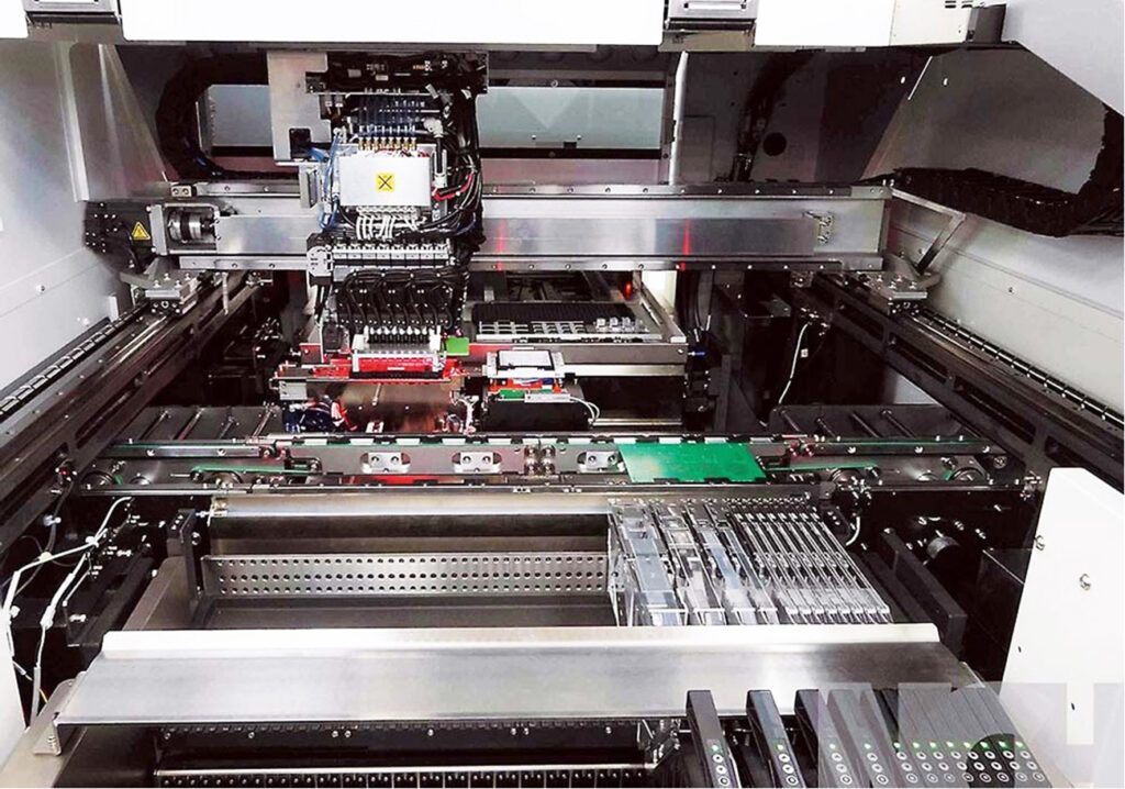
Integration of Back-end, SMT Processes
In the back end of the semiconductor manufacturing process, packaging technologies such as System in Package (SiP), three-dimensional (3D) packaging and chiplet technology, are emerging. 3D packaging technology is used to connect the chips to the substrate. In 3D packaging, multiple chips such as memory and microcontrollers are stacked in a package in 3D orientation. Meanwhile, in chiplet technology, chips are manufactured and integrated using different process nodes.
Specifically, flip chip mounting, which uses through-silicon vias (TSVs) and bumps (solder balls) to connect to the substrate, is expanding for 3D mounting. Meanwhile, multi-chip modules (MCM), in which multiple bare chips and passive components are mounted and packaged as a single IC, are also on the rise.
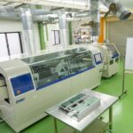
Recently, the back-end semiconductor manufacturing process and the electronic component mounting process are becoming more seamless. As the mounted components become smaller and the number of semiconductor devices increases, the need for a mounting process that is close to the bonding process is also increasing. Thus, SMT is increasingly being applied to these bonding processes.
Mounting equipment manufacturers are focusing on these trends. Further, SMT companies are expanding their product lineups eyeing the integration of SMT and semiconductor manufacturing processes. Also, they pursue commercialization through mergers and acquisitions.
In August 2018, FUJI Corporation acquired all shares of FASFORD Technology Co., Ltd. (FFT), a semiconductor manufacturing equipment manufacturer that focuses on die bonding equipment. The new company was created to promote collaboration between FUJI’s proprietary technologies cultivated in electronic component mounting robots and FFT’s semiconductor-related technologies.
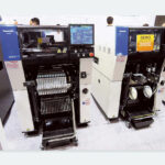
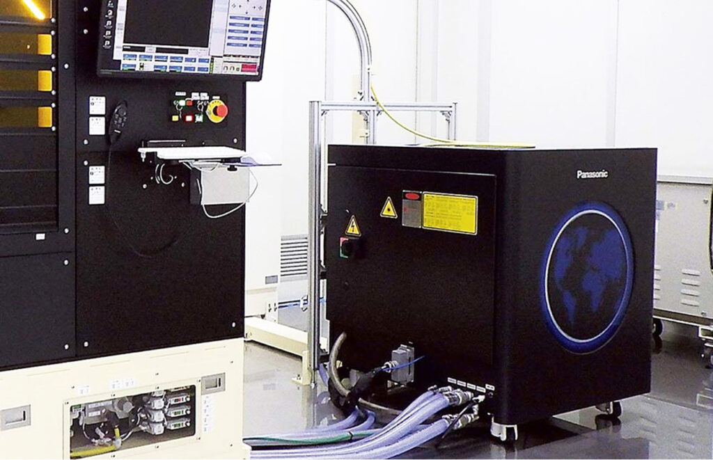
Process Automation Business Division, Panasonic Connect Co., Ltd. specializes in circuit formation processes. These include electronic component mounting machines, semiconductor manufacturing equipment, display manufacturing equipment, and software; thermal processing systems, like welding machines; and electronic component mounting machines, including semiconductor manufacturing equipment, display manufacturing equipment, and software. The company pioneered the production of dry etch systems, plasma dicers, LCD bonders, die bonders, flip chip bonders, and other products in the chip packaging industry.
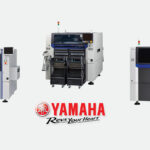
Meanwhile, Yamaha Motor Co., Ltd. is the parent company of Yamaha Robotics Holdings Co., Ltd. (YRH), which handles Yamaha’s semiconductor manufacturing equipment business. Launched in July 2019, YRH was created through the integration of SHINKAWA Ltd., whose main business is semiconductor bonding; APIC YAMADA Corporation, a molding equipment manufacturer; and PFA Corporation, a semiconductor inspection equipment manufacturer. YRH aims to provide a one-stop smart solution by linking semiconductor back-end processes and SMT processes.
JUKI Corporation had formed a capital and business alliance with AI Mechatec, a flat panel display (FPD) manufacturing equipment and semiconductor package manufacturing equipment company. It aims also to integrate its semiconductor back-end processes and SMT processes.
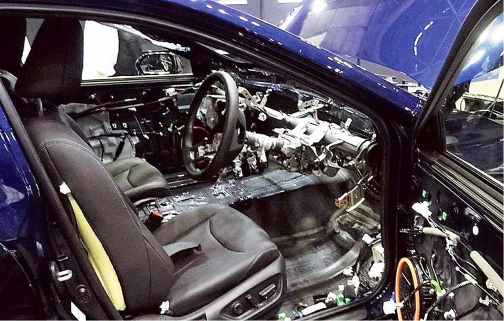
Innovations Surrounding Lightweight EVs
In response to global environmental issues, the shift to the adoption of EVs has been progressing worldwide. As EVs require less energy to run long distances, weight reduction has become important. Accordingly, manufacturers are scrambling to develop materials and processing technologies to reduce the weight of vehicles.
In terms of structural materials, high-tensile steel sheets are being used with thinner wall thicknesses to reduce weight. To manufacture high-tensile steel sheets, elements such as carbon, nickel, silicon, and manganese are added in very small quantities to iron. This process increases the strength through microstructure control.
Aluminum, which is lighter than steel, is also increasingly used for engine components such as cylinders, and for exterior panels such as bumper beams, doors, and roofs. The use of magnesium, which is even lighter than aluminum and is currently used in aircraft and rockets, is also expanding.
Moreover, interior parts such as instrument panels and functional parts such as motor housings are increasingly replacing metals with resins such as polypropylene to reduce weight. Polypropylene is suitable for automotive interior parts and electrical components because of its excellent balance of mechanical properties and moldability, as well as its low specific gravity.
Meanwhile, carbon fiber reinforced plastic (CFRP), a composite material made by reinforcing resin with carbon fiber, is also expected to be used in EVs, but the processing technology is challenging, and its full-scale adoption is still in the research stage, including productivity. Research is also underway to apply plant-derived and other biomass plastics to EVs. However, strength and heat resistance are issues that need to be addressed before they are used in EV parts.
Processing technologies are evolving in line with the development of materials for EVs.
For the adhesion of resins used in EVs, a method that improves adhesion performance by modifying the surface is attracting attention. Specifically, surface modification is a process that forms an adsorption layer with strong intermolecular forces on the surface of the adherend material. Also, other methods such as irradiating the surface with short-wavelength ultraviolet light or irradiating with plasma, both of which can be performed in the air, are available. Specifically, plasma irradiation is a surface modification technique that utilizes the electrically neutral radical properties of plasma. Plasma has a low temperature of irradiated gas and can remove organic contaminants, modify the surface, and improve the adhesive strength of heat-sensitive rubber and resin without causing deterioration of the materials.
Magnesium is considered a relatively weldable metal, but it easily forms oxide film, and the melting point of the oxide film is very high at 2,500ºC, which hinders welding processes. For this reason, spot welding, which uses electrical resistance when pressure is applied, and intense laser beams are used for welding.
Laser processing machines are widely used in EV material processing, and blue laser processing is attracting attention in copper processing for EV motors and batteries. The spread of EVs is accelerating technological innovation in material processing.
- Share: