ASIA ELECTRONICS INDUSTRYYOUR WINDOW TO SMART MANUFACTURING
India Executes Semiconductor Policy Into Full‑Stack Growth
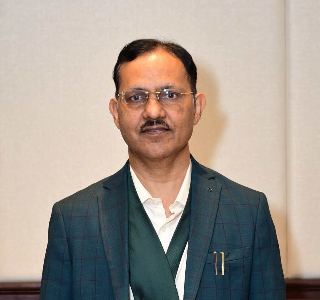
In this exclusive interview, IESA and SEMI India President Ashok Chandak explains how policy momentum is translating into manufacturing reality, capital efficiency, and long‑term ecosystem competitiveness—and why global chipmakers are starting to take India seriously now.
For many decades, India’s role in the global semiconductor industry was anchored in its powerhouse engineering talent and design capabilities. Today, that role is deliberately evolving with the rise of domestic semiconductor fabs.
India is no longer positioning itself solely as a design hub or a large consumption market. Instead, it is undertaking a decisive transition towards a full-stack electronics and semiconductor ecosystem, carving its own relevance in global manufacturing and supply chains.
Thanks to sound government initiatives, such as the India Semiconductor Mission (ISM), Production Linked Incentives (PLI), and the Electronic Component Manufacturing Scheme (ECMS), India is now translating these policies into actual fabs, OSATs, components manufacturing facilities, and other infrastructure. The country’s roadmap now emphasizes high volume semiconductor nodes, packaging, and other value addition activities while further leveraging its advanced capabilities in design, R&D, and IP creation.
Clearly, India’s semiconductor industry has moved from being a participant to becoming a structural player in the semiconductor ecosystem.
In this interview with AEI, Ashok Chandak, President of the India Electronics and Semiconductor Association (IESA) and SEMI India offers an industry-level perspective on India’s progress, priorities, and remaining challenges as the country enters the next phase of semiconductor development.
AEI: India’s electronics and semiconductor sectors have advanced rapidly in recent years. How would you describe the current industry environment?
Chandak: India has moved very fast over the last few years in both semiconductors and electronics. From a high‑level perspective, two important things stand out: trustworthiness and India becoming a serious investment destination. India is demonstrating capability and competence.
“India is now moving from being primarily a semiconductor design hub to becoming a full‑stack semiconductor and electronics ecosystem.”
Ashok Chandak, President, IESA
The next phase is about scaling up and execution. The government, both central and state, is very supportive with a multitude of policies. Industry interest is strong—not only to serve domestic markets but also to position India as an important player in the global supply and value chains.
India is now moving from being primarily a semiconductor design hub to becoming a full‑stack semiconductor and electronics ecosystem spanning design, manufacturing, packaging, systems, and advanced applications.
AEI: IESA recently announced the IDSPS division. How will this support the industry in the long term?
Chandak: The Indian Design, Semiconductors, Packaging, and Systems (IDSPS) division focuses on R&D, which is essential for the future. While India has a strong design talent base, R&D for product creation and manufacturing technology must grow.
IDSPS will help India move beyond design services toward IP creation and manufacturing technology development, which is critical for long‑term sustainability.
AEI: How did ISM 1.0 create a multiplier effect on private‑sector investment?
Chandak: The ₹76,000 crore (US$10 billion) allocation under ISM 1.0 was designed to catalyze a multiplier effect. Semiconductor manufacturing typically attracts three to five times private investment in allied industries.
With fabs approved, supporting infrastructure—logistics, ports, roadways, warehousing—is developing. OSATs are entering production, and manpower demand is rising. ISM 1.0 has triggered multiple fab and OSAT projects. There are almost 10 projects approved by the central government and four to five more by state governments.
Overall, ISM 1.0 has acted as a strategic catalyst, anchoring a new industrial sector and accelerating ecosystem momentum.
AEI: What is the essence of ISM 2.0, and why is it the logical next step?
Chandak: Semiconductors are long‑term ventures. ISM 2.0 reflects the government’s commitment to build on the foundation created by ISM 1.0.
ISM 2.0 supports the entire ecosystem, including materials, specialty chemicals, gases, and equipment. It will expand packaging and OSAT capabilities, strengthen compound semiconductors, and accelerate AI, automotive, and power electronics chips. Overall, ISM 2.0 will help India move from being a participant to a structural player in the global value chain, shifting from project‑based incentives to ecosystem competitiveness.
AEI: How realistic is India’s roadmap toward 3nm and 2nm nodes?
Chandak: India’s aspiration toward 3nm and 2nm should be viewed as a long‑term goal. While it is not part of the immediate ISM 2.0 focus, India already has design centers working on 3nm and 2nm chips for global companies.
Manufacturing at these nodes is a long‑term aspiration. Currently, India’s focus on 28nm to 120nm is appropriate, as these nodes represent the highest global volumes. Jumping directly from 28nm to 2nm is not a practical approach.
AEI: How has India’s reliance on electronics imports changed?
Chandak: In FY2024–25, India’s electronics demand was US$196 billion, with domestic production at US$138 billion—a gap of about 30 percent. Five years ago, the gap was around 50 percent. Exports are also growing.
The only challenge is we continue to import many components and semiconductors. However, I see it is going to change over the next 12 to 14 months as 46 ECMS projects worth ₹22,000 crore come online, producing capacitors, connectors, PCBs, and display modules. Additionally, four OSATs are expected to be operational by the end of the year, improving localization, cost effectiveness, and value addition.
AEI: What is the ideal balance between domestic production, imports, and exports?
Chandak: It is not necessary to produce everything domestically. The plan is producing 70–80 percent of demand locally is a good target, while exports are critical for scalable, sustainable manufacturing. By 2030, around 25 percent of production could be exported, about 20 percent of demand imported, and the remainder consumed domestically.
AEI: Beyond infrastructure, what challenges must India address to ensure smooth ecosystem operations?
Chandak: Infrastructure challenges will be addressed over time. The more critical issues are talent readiness, regulatory efficiency, and execution. Manufacturing talent—particularly for fabs, OSATs, and electronics manufacturing—needs further upskilling. Regulatory processes across departments must be more coordinated to enable faster approvals. Execution and local development of supply chains for specialty gases and chemicals are also essential.
“India’s goal is not just to build fabs, but to build a long‑term ecosystem that powers the digital economy.”
AEI: SEMI said semiconductor market could reach US$2 trillion by 2035. What share of the global market India targets to carve out realistically?
Chandak: By 2030, India’s semiconductor demand is projected at about US$103 billion. While we have not estimated 2035 in detail, demand could exceed US$250 billion. Realistically, India could target 10–15% participation in the global value chain by combining design strength, IP creation, manufacturing, and packaging.
AEI: What is the industry outlook once capital subsidies wind down?
Chandak: Subsidies are important to bridge initial capability gaps, but the long‑term goal is a self‑sustaining industry. This depends on scaling electronics manufacturing, aligning semiconductor production with domestic demand, and expanding exports. Innovation, product design, and deep integration into the global semiconductor value chain are critical. Strategic trade agreements and global partnerships will also play a key role.
Ultimately, India’s focus is not just building fabs, but building a long‑term ecosystem to power the digital economy of the future.
27 March 2026
Cristian Canoza
- Share: