


ASIA ELECTRONICS INDUSTRYYOUR WINDOW TO SMART MANUFACTURING
Applied Materials Reinvents AI Chip R&D With New EPIC
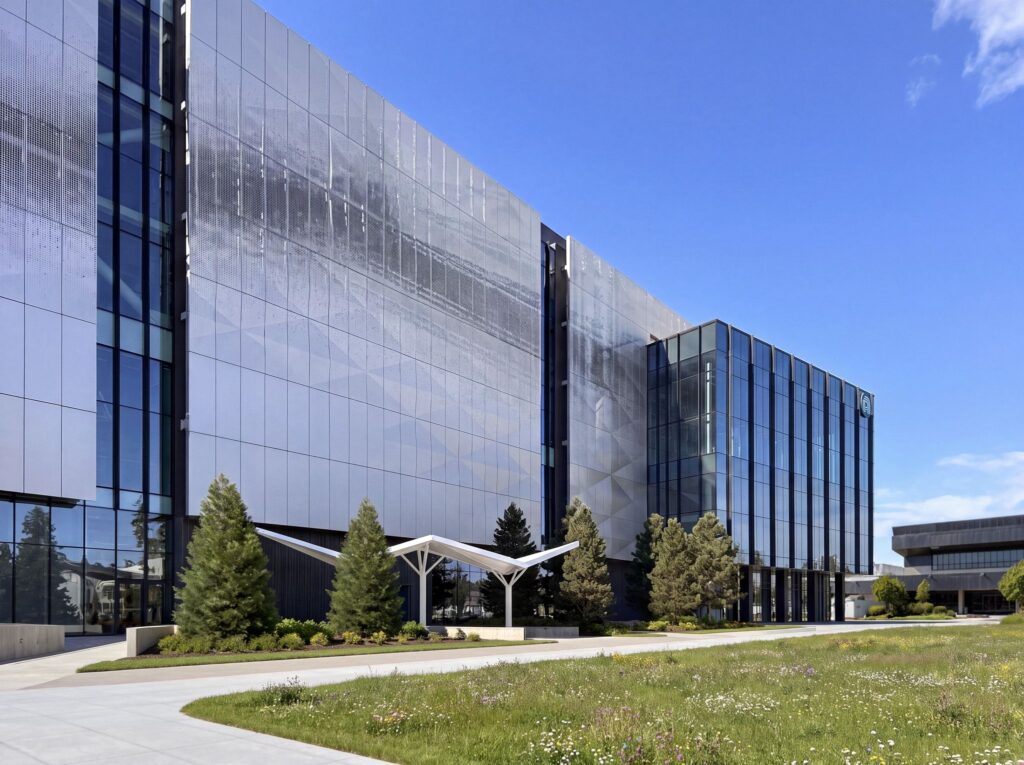
Applied Materials has opened its US$5 billion EPIC Center in Silicon Valley, advancing a new approach to semiconductor research and development that brings chipmakers, equipment suppliers, researchers and academic institutions together to accelerate the path from innovation to manufacturing.
For the semiconductor industry, the significance extends beyond the scale of the facility. The EPIC Center is designed to address one of the industry’s growing challenges: aligning increasingly rapid AI-driven product cycles with technology development processes that can take years to reach production.
Gary Dickerson, chairman and CEO of Applied Materials, said the facility is intended to “dramatically accelerate the path from materials innovation to high-volume manufacturing” by enabling closer collaboration among leading chipmakers, systems companies, equipment partners and researchers.
Ecosystem Collaboration Moves to the Forefront
The center’s founding partners include major semiconductor manufacturers and technology companies such as TSMC, Intel, Samsung, Micron and SK hynix, alongside a broader network of industry and academic collaborators.
Applied said the EPIC model replaces traditional sequential development processes with parallel innovation, allowing participants to shorten learning cycles and gain earlier access to emerging process technologies and manufacturing solutions.
Dickerson emphasized the strategic importance of development speed, stating: “There are five to 10 key technologies that determine performance and yield. It’s all about, how do we accelerate all of that? The goal here is to cut that whole cycle time at least 30%, improving the time to market.”
Focused on Future Generations of AI Computing
The EPIC Center is expected to support development efforts several technology generations ahead of current production, reflecting increasing industry focus on advanced materials, process technologies and energy-efficient computing architectures required for future AI systems.
“We’re working four generations ahead of time,” Dickerson said. “Whoever brings those innovations to market fastest is going to win.”
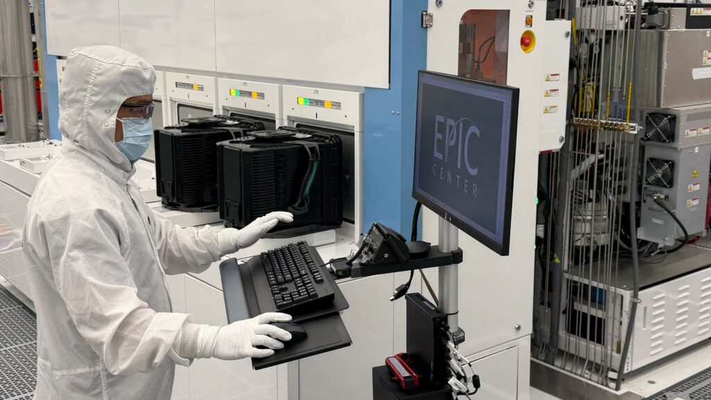
The facility includes approximately 600,000 square feet of research space and more than 180,000 square feet of cleanroom capacity dedicated to collaborative semiconductor process and equipment development.
For industry executives, the broader message is clear: as AI drives greater complexity across semiconductor manufacturing, competitive advantage may increasingly depend not only on technology leadership, but also on the industry’s ability to innovate collectively and commercialize breakthroughs faster.
13 October 2026
- Share: