ASIA ELECTRONICS INDUSTRYYOUR WINDOW TO SMART MANUFACTURING
Unique IC Processes Emerge to Create New Businesses
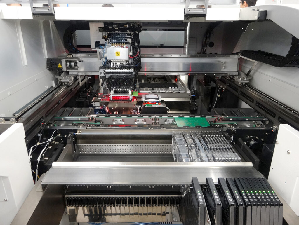
The integration of semiconductor manufacturing processes and the surface mount technology (SMT) is progressing. Furthermore, mounting machine companies are advancing full-scale commercialization in new areas.
Behind this is the evolution of mounting processes, which is gathering speed. This includes development and diversification of bonding and packaging technologies of semiconductor manufacturers. Of course, the mixed mounting of semiconductor devices and electronic components manufactured by different processes.
The semiconductor manufacturing process has two parts, and they are pre-process and the post-process. In the pre-process, the finished wafer turns into a chip (die) based on the circuit design and pattern design. Meanwhile, in the post-process, the chip separated from the wafer (dicing) fixes to the lead frame with a bonder. Hence, the electrode of the chip and the lead frame connects with metal wiring using a wire bonder or a flip chip bonder. Resin then acts as a package of the whole device.
New Packaging Technologies
The amount of digital data processed by semiconductor devices has increased as for 5G, for example. In addition, the high integration has advanced by miniaturization according to “Moore’s Law”.
However, miniaturization requires enormous development and manufacturing costs. Therefore, semiconductor manufacturers are trying to achieve higher integration by using new packaging technologies. One example is 3D mounting. This is the stacking and mounting of multiple chips, such as memories and microcomputers, in 3D directions in a package, or also known as system-in-package (SiP). Another is the chiplet technology, which integrates into a single package manufactured chips using different process.
In 3D mounting, the flip mounting using through-silicon via (TSV) and bumps (solder balls) for connection with a board is becoming more popular. In addition, multi-chip modules (MCMs) are increasing in number, in which several multiple bare chips and passive components are mounted onto a single IC. These manufacturing processes increasingly require the SMT bonding technology.
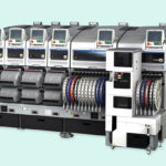
Currently, in EMS, different factories and production lines perform the process of mounting flip chip devices and the SMT process. Recently, however, these processes are performed on the same factory floor or on the same production line for the purpose of improving the production efficiency, increasing the need for the integration of different equipment. Mounting machine companies are carefully watching the trends of these semiconductor manufacturers and production sites.
Role of Bonding Companies
In August 2018, FUJI Corporation acquired all shares of Fasford Technology Co., Ltd. (FFT), a manufacturer of semiconductor production equipment specializing in die bonding equipment. The acquisition amount totaled ¥21.8 billion.
Hiroyuki Ao, General Manager and Technology Planning Manager, Sales Engineering Department, Robotics Solutions Division, said demand for die bonders is growing. Hence, the performance of FFT, to which he is also a director, is growing significantly as well.
“The fusion of the semiconductor mounting technology of FFT and the SMT technology of FUJI Corporation, has led us to develop equipment for new business areas, such as mixed mounting of chiplets.”
Connecting Post-Process, SMT
Yamaha Motor Co., Ltd. established in July 2019 Yamaha Robotics Holdings Co., Ltd. Moreover, the aim is to provide a one-stop smart solution by combining the semiconductor post-process and the SMT process.
The new company integrates the businesses of IC bonding company SHINKAWA Ltd., molding equipment supplier APIC YAMADA Corporation, and SHINKAWA subsidiary PFA Corporation.
Ayako Egashira, Executive General Manager of Robotics Business Unit, Solution Business Operations said they have been expanding their business and focus on creating an SMT line under the Yamaha brand as a feature of our company.
“In the future, we will add FA and the post-process for semiconductor manufacturing to SMT. In addition, we will promote a one-stop solution with a view to labor savings and optimization of the entire factory,” said Egashira.
Panasonic Smart Factory Solutions Co., Ltd. is promoting process innovation in the industry, based on two global businesses. They are the circuit formation process, which includes semiconductor manufacturing equipment, display manufacturing equipment, electronic component mounting machine, and software, and the thermal processing system, including welding machine, welding robot, and laser processing robot. It has commercialized dry etchers, plasma dicers, liquid crystal bonders, die bonders, flip chip bonders, etc., for the semiconductor manufacturing process.
- Share: