ASIA ELECTRONICS INDUSTRYYOUR WINDOW TO SMART MANUFACTURING
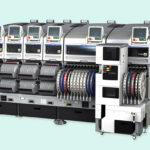
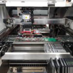
FUJI’s Novel Mounting Tools Target New Fields
FUJI Corporation has been advancing the commercialization of equipment in the new areas. Particularly, the company looks at opportunities in semiconductor back-end process technology and electronic components mounting technology.
Consequently, FUJI targets full-fledged business development with Fasford Technology Co., Ltd. Headquartered in Japan’s Yamanashi, Fasford Technology is a semiconductor manufacturing equipment manufacturer FUJI adopted as a subsidiary in 2018.
The fusion between the semiconductor manufacturing process and surface mount technology (SMT) has been progressing. These include the development and diversification of bonding and packaging technologies by semiconductor manufacturers. Meanwhile, the same is true for mixed mounting of semiconductor devices and electronic components, which various processes have produced.
FUJI focuses attention on the semiconductor market that will grow even further in the future in a wide range of fields. These include artificial intelligence (AI), autonomous driving, communications, and industrial equipment.
Complements Growing IC Market
In acquiring Fasford Technology at ¥21.8 billion (US$188.65 million), FUJI aims to strengthen solutions for entire production line. This encompasses semiconductor backend processes and electronic components mounting processes. In addition, the company also wants to fortify its capability to propose next-generation technologies.
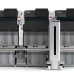
Founded in 1963 as Ome Electronics Kogyousho Co., Ltd., the back-end processes group of the Semiconductor Division of Hitachi, Ltd., Fasford Technology develops and manufactures die bonding equipment.
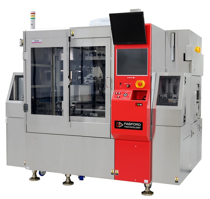
A die bonder attaches dies diced from wafers on printed circuit boards (PCBs) and house them in packages. Moreover, Fasford Technology has original technologies, including a technology to handle thin dies 25 to 50μm. This is without imposing stress by supporting them from the bottom upon pick up by vacuum suction. It also has a technology to laminate many thin dies.
Particularly, the company has in its lineup the DB850, DB830plus+, and DD100 Series die bonders equipped with these technologies. Furthermore, manufacturing process of NAND flash memories and low-power DRAMs (LPDRAMs) require these bonders.
Hiroyuki Ao, General Manager/Technology Planning Manager, Sales Engineering Dept., Robotics Solutions Div. of FUJI, who is also Director of Fasford Technology, noted the expansion of the semiconductor market. “With the expansion of the semiconductor market, the demand for die bonders has been increasing and the business performance of Fasford Technology has also been remarkably growing,” said Ao.
Creates New Values
Ao added Fasford Technology owns an excellent technology to pick up dies and mount them on PCBs. Especially, it has an 80 percent share for equipment for NAND flash memories. Bonding technology has close relations with SMT.
“We combine our company’s original technologies we have nurtured in the production of electronic components mounting robots and Fasford Technology’s semiconductor-related technologies. Together, we have been developing products that create new values in new business areas that stride the two fields. We strengthen total capabilities to make proposals as a mounting robot manufacturer and a semiconductor manufacturing equipment manufacturer,” said Ao.
Since 2018 when FUJI made Fasford Technology its subsidiary. Hence, the companies have promoted exchanges on technological front, including personnel exchanges, thereby enhancing synergetic effect. By the end of the fiscal year, the companies plan to commercialize a product in the new field, which combines FUJI’s high-speed transfer technology and Fasford Technology’s die pickup technology.
- Share: