


ASIA ELECTRONICS INDUSTRYYOUR WINDOW TO SMART MANUFACTURING
Applied, Intel Expand Alliance for AI Chipmaking
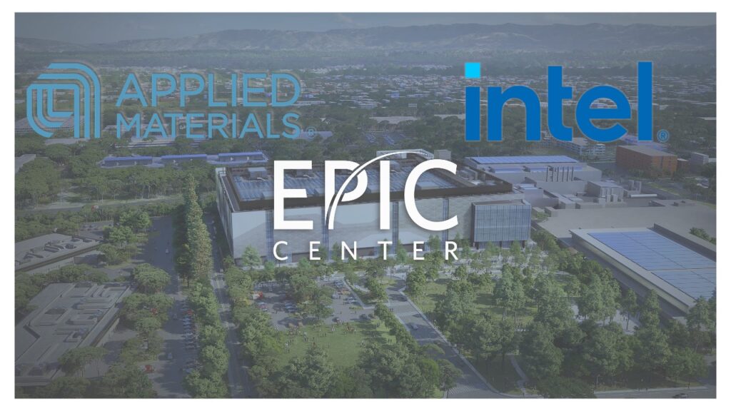
Applied Materials and Intel are expanding their long-standing collaboration to accelerate the development of next-generation semiconductor technologies critical to artificial intelligence computing. The initiative combines resources from Applied Materials’ new EPIC Center in Silicon Valley and Intel’s research and development campus in Hillsboro, Oregon, with the goal of shortening the path from research breakthroughs to high-volume manufacturing.
The collaboration will focus on key technology building blocks that increasingly determine AI system performance, including advanced transistors, interconnects and packaging solutions. As demand for AI infrastructure continues to grow, chipmakers face mounting pressure to deliver higher performance, improved power efficiency and greater system-level integration.
“Applied and Intel share a decades-long history of deep collaboration focused on pushing the boundaries of materials engineering to advance the semiconductor roadmap,” said Gary Dickerson, President and CEO of Applied Materials. “Bringing our teams together at the EPIC Center will deepen that partnership and accelerate the transistor, interconnect and packaging innovations needed to drive the future of AI computing.”
Drive Need for New Device, Packaging Architectures
According to the companies, joint development efforts will include next-generation materials, process technologies and device architectures for advanced logic nodes targeting AI workloads. The work spans both front-end semiconductor processes and back-end interconnect scaling technologies.
A major focus will be advanced packaging for Intel’s Foveros-based 3D stacking technology. The companies aim to support higher interconnect density, stronger power delivery and improved thermal management, all of which are increasingly important for high-performance computing platforms designed to handle emerging agentic AI workloads.
“The demand for AI computing is driving the need for major advances in performance, power efficiency, and packaging,” said Lip-Bu Tan, CEO of Intel. “Applied Materials is an important partner, and we look forward to expanding our work together at the EPIC Center to help accelerate the path from the lab to high-volume manufacturing in the United States.”
EPIC Center Positioned as Industry Co-Innovation Hub
The partnership also underscores the strategic role of Applied Materials’ EPIC, or Equipment and Process Innovation and Commercialization, Center. Scheduled to become operationally ready this year, the facility is designed to reduce commercialization timelines by providing customers earlier access to research programs, faster learning cycles and more rapid technology transfer into manufacturing environments.
For both companies, deeper collaboration is increasingly viewed as a necessity as semiconductor scaling challenges become more complex with every process generation.
“Accelerating our R&D to keep pace with the rapid buildout of AI infrastructure is critical to delivering the technology, manufacturing excellence and foundry services our customers expect from Intel Foundry,” said Naga Chandrasekaran, Executive Vice President, Chief Technology and Operations Officer and General Manager of Intel Foundry. “Applied Materials’ new EPIC Center provides an environment where our teams can collaborate even more closely and at higher velocity to accelerate materials development and process innovations.”
The expanded alliance highlights how ecosystem-wide collaboration is becoming central to advancing AI-era semiconductor innovation, particularly in areas where materials engineering, process integration and advanced packaging increasingly intersect.
08 October 2026
- Share: